Nixie · Volume 6
Build It Yourself — the ATMega Cool Nixie Clock
From the owned design files to a glowing clock: schematic, BOM, PCB, firmware, bring-up, calibration
This is the volume the rest of the series has been pointing at. Vol 2 covered the nixie tube and its strike-and-maintain voltages; Vol 3 built the ~180 V boost supply; Vol 4 laid out the drivers from the classic 74141 to HV shift registers; Vol 5 covered the timebase. Here all four come together into one buildable object — the ATMega Cool Nixie Clock, the design this hub holds on disk, with a real schematic, a PCB layout, and working firmware for Telefunken ZM1210 tubes. This volume walks the design block by block, gives a buildable bill of materials with values and units, takes the gerbers to a board house and the enclosure to Jeff’s lab, flashes the firmware over ISP, and brings the whole thing up in the only safe order — low-voltage logic first, the ~180 V rail second on a current-limited bench supply, tubes last. Read Vol 10 before you energize anything in § 6.6: everything past the boost inductor is at a voltage that can hurt you.
A word on what “the design” means, because the folder holds a small family rather than one monolithic board. Two concrete realizations sit side by side on disk:
- a static-drive ZM1210 board (
zm1210-display-atm-7.sch) — an AVR feeding one 74141 BCD-to-decimal decoder per tube, with an onboard boost supply built around an IRFR320 MOSFET and a BYV27 rectifier; and - a multiplexed firmware,
nix-in-17(Henry Carl Ott, N2RVQ, 2005) — an ATmega48 that anode-multiplexes four tubes over ten shared cathode lines and generates the high voltage in software by PWM-ing the boost MOSFET against an ADC feedback sample.
Both are “the build.” The static board leads the BOM and schematic walk because it is the easier one to understand; the multiplexed firmware actually runs and is the richest source of concrete numbers (HV set-points, the cathode anti-poisoning routine, the leading-zero rule). Where they diverge — direct-drive vs. multiplex — the difference is exactly the Vol 4 trade, made explicit in § 6.1.3.
6.1 Design overview
6.1.1 The signal chain
At block level the clock is the four-subsystem machine of Vol 1, wired in series from a 12 V brick to a glowing numeral:
  12 V DC in
     │
     ├─[ 7805 ]──► +5 V logic rail ──┬──► AVR MCU (ATmega48 / AT90S4433-class)
     │                               │      ├─ timebase: 32.768 kHz xtal on Timer2 (async)
     │                               │      │           OR onboard DS3231/DS1307 RTC
     │                               │      ├─ 2 buttons: MODE (set) + INC
     │                               │      └─ HV control + feedback
     │                               │
     │   ┌───────────────────────────┘
     │   │  BCD digit data
     │   ▼
     │  74141 BCD→decimal HV drivers (one per tube, static)   ◄── Vol 4
     │   │   (or: 74HC595 shift chain feeding the 74141s)
     │   ▼
     │  ZM1210 nixie tubes ── cathode pulled to ~0 V lights that numeral
     │       ▲
     │       │ anode (~180 V) through anode resistor R_a
     └─[ BOOST: IRFR320 switch + 100 µH + BYV27 → ~180 V ]──┘   ◄── Vol 3
              ▲
              └─ PWM gate drive + HV_SENSE ADC feedback (software-regulated)
The boost supply (Vol 3) lifts 12 V to the ~180 V anode rail; the AVR keeps time (Vol 5) and decides which cathode to ground; the drivers (Vol 4) do the grounding while standing off the anode voltage on the nine cathodes they are not lighting; the tubes (Vol 2) glow. The only hard parts are the two in the HV path — making ~180 V cleanly and switching it without frying a logic pin — and those are where this volume spends its care.
6.1.2 The design files on disk
Everything below is grounded in the files actually present in
02-inputs/ATMega Based Cool Nixie Clock/. It is worth listing them, because together they
are a complete, reproducible design and a reader should know which file answers which
question:
Table 1 — question
| File | What it is | What it grounds |
|---|---|---|
zm1210-display-atm-7.sch | EAGLE schematic of the ZM1210 static-drive display board | The 74141 drivers, ZM1210 tubes, IRFR320 boost MOSFET, BYV27 rectifier, 100 µH inductor, 7805, 4.096 MHz crystal, AT90S4433 MCU |
nix-in-17_1_1.zip → nixie_in17.asm | The working AVR firmware (ATmega48, AVR assembly) | HV PWM/feedback set-points, anode-multiplex scan, cathode-saver, 12/24 + leading-zero behaviour, the two-button UI |
nix-in-17_schematic_1_1.pdf | Schematic matching the nix-in-17 firmware | Multiplexed direct-drive cathode wiring (image-only PDF) |
2D3 Nixie clock Schematic (Multiplexed).pdf | A multiplexed variant schematic | The multiplex alternative to static 74141 drive |
nixiepcb.zip | PCB package: Schematic.pdf, pcb_layput.pdf, Layout_Options.pdf, Voltage_options.pdf | The board artwork and HV/layout option notes |
nixcct.pdf | A mains-derived (~230 V line) nixie supply reference | An alternative, line-derived HV approach (115/230 VAC, 1N4005, 4013 divider, NE-2 indicator) |
74HC_HCT595.pdf | 74HC/HCT595 shift-register datasheet | The shift-register expansion path (drive many 74141s from few MCU pins) |
ATMegaManual.pdf | The ATmega datasheet | MCU peripherals, fuse map |
AtmelInSystemProgramming.pdf | AVR910 In-System Programming app-note | The 3-wire SPI ISP procedure used in § 6.5 |
seconds.pdf | Seconds-display add-on schematic | The 6-digit (HH:MM:SS) expansion option |
img_4090.jpg, img_4091.jpg, img_4101.jpg | Owner build photos of a finished unit | Figure slots throughout this volume |
6.1.3 Direct-drive vs. the multiplexed variant
The single most important architectural choice in a nixie clock — and the one the two on-disk designs split on — is static (direct) drive vs. multiplexing. It is the Vol 4 trade made concrete:
- Static drive (the
zm1210-display-atm-7board): every tube has its own dedicated 74141 decoder permanently connected to its ten cathodes. All four digits are lit continuously. The cost is parts — one 74141 per tube, and enough MCU pins or shift registers to feed 4 × 4 = 16 BCD lines — but the reward is the brightest, steadiest, flicker-free display, with each cathode running at a calm few milliamps set purely by its anode resistor. - Multiplexing (the
nix-in-17firmware and the2D3variant): the ten cathodes are shared across all four tubes (one common bus of ten lines), and the firmware lights one digit at a time by switching that digit’s anode on for its slice of a fast scan, then moving to the next. The firmware’sscanroutine does exactly this — it drives the shared cathode pattern, then pulsesANODE_HH,ANODE_H,ANODE_M,ANODE_MMin turn. The reward is a dramatic parts saving (ten cathode drivers total instead of forty, no per-tube decoder), at the cost of (a) a refresh fast enough to beat visible flicker and (b) higher peak cathode current to keep average brightness up at a 1/4 duty cycle — which feeds straight into the anode-resistor sizing in § 6.3.
The honest recommendation: build the static ZM1210 board for the best-looking clock if
you don’t mind the extra 74141s, and study the multiplexed firmware to see how few parts
a nixie clock can be reduced to. The schematic walk leads with the static board (it maps
one-to-one onto Vol 4); the multiplex specifics return in § 6.5, where nix-in-17 is the
authority.
6.2 Schematic walk
This section walks the zm1210-display-atm-7 display board (the EAGLE schematic on
disk) block by block, then notes where the multiplexed nix-in-17 schematic differs. The
schematic files are image-only PDFs / EAGLE binaries, so they are referenced as figure
slots rather than reproduced; the part values quoted below are read directly out of the
EAGLE file’s part list (74141N, IRFR320, BYV27, 100uH, 4.096MHz, 7805,
ZM1210/12, AT90S4433).
6.2.1 The display board and tubes
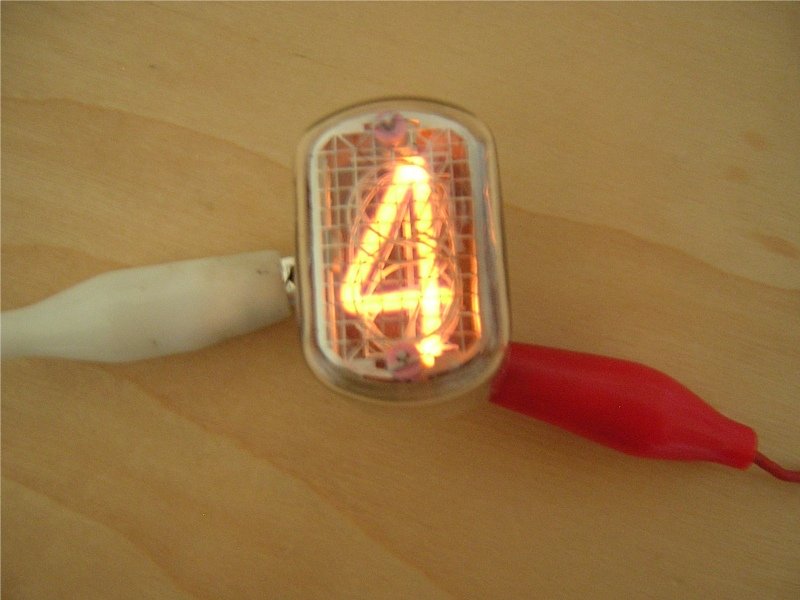
The four ZM1210 tubes are the reason for everything else. The ZM1210 is an end-view
Telefunken tube (15.5 mm digit height, Vol 1’s tube table) with a wire anode mesh and a
stack of ten numeral cathodes. On the static board each tube’s anode goes up to the ~180 V
rail through its own anode resistor (the current-limiting resistor of Vol 2), and each
of its ten cathodes lands on the matching output of that tube’s 74141. Light a cathode by
pulling it to ground and the numeral over it glows; the other nine cathodes float at or
near the anode rail and stay dark. The decimal-point / “PM” indicator (the firmware’s
K_PM line) is wired the same way as an eleventh cathode where the tube or board provides
one.
6.2.2 The driver chain — how BCD reaches each 74141
The 74141 (and its Soviet clone, the K155ID1) is the canonical nixie driver of Vol 4: a BCD-to-decimal decoder whose ten outputs are open high-voltage transistors rated to stand off the anode rail. You present a 4-bit BCD code (0000–1001) on its A/B/C/D inputs and it pulls exactly one of its ten outputs (and therefore one cathode) to ground, holding off the ~180 V on the other nine. One 74141 fully drives one tube.
That leaves the wiring question: four tubes need 4 × 4 = 16 BCD lines, more than a small AVR like the AT90S4433 has spare. The board has two ways to solve it, and both are represented on disk:
- Parallel from the MCU. If enough port pins are free, the four BCD nibbles are driven directly. This is simplest but pin-hungry.
- 74HC595 shift-register expansion. The
74HC_HCT595datasheet is in the folder for exactly this reason: a chain of serial-in/parallel-out shift registers lets the MCU clock all 16 BCD bits out over just three pins (data, clock, latch), the registers holding the BCD code steady on the 74141 inputs while the MCU does other work. Two 8-bit ‘595s carry all four nibbles. This is the “74HC595 shift chain → 74141” topology the hub overview (Vol 1) describes, and it is the recommended way to keep the static board’s pin count sane.
The multiplexed nix-in-17 design takes neither path: it drops the 74141s entirely and
drives the ten shared cathode lines directly from MCU port pins (firmware bits
K_0…K_9 spread across PORTB/PORTC/PORTD), each cathode line buffered — per the
nix-in-17 schematic — by a high-voltage switching transistor that can pull a cathode to
ground while standing off the ~180 V on the active tube. Trading forty driver outputs for
ten is the whole point of multiplexing.
6.2.3 The HV boost section
This is the dangerous block and the most interesting one. The static board carries an onboard step-up (boost) converter that makes the ~180 V anode rail from the 12 V input — the same architecture as Vol 3’s low-voltage-derived supply, scaled down for nixies. Per the schematic’s part list it is built from:
- L1 — a 100 µH inductor, the energy-storage element;
- Q (IRFR320) — an N-channel MOSFET (≈400 V drain rating), the switch that chops current through the inductor;
- D (BYV27) — a fast-recovery rectifier, which catches the inductor’s flyback pulse and charges the reservoir cap; a slow 1N400x will not switch fast enough here;
- a reservoir / filter capacitor rated comfortably above the output (≈10–47 µF at ≥250 V — never a 200 V part on a 180 V rail);
- a feedback divider from the HV output down to a few volts, sensed by the MCU’s ADC; and
- a bleeder resistor permanently across the output cap (Vol 3, Vol 10) so the rail self-discharges after power-off.
   +12V ──[L1 100µH]──┬──|>|── D (BYV27) ──┬───────────► ~180V anode rail
                      │                     │
                  Q drain (IRFR320)      C_res (≥250V)         ┌─ R_top
                      │                     │                  │
   PWM gate ──[Rg]── Q gate                GND ── R_bleed     HV_SENSE ◄─┤ (ADC)
   from MCU            │                                      divider    │
   (OC0B)           Q source ── R_sense ── GND                          R_bot ─ GND
What makes this elegant is that the regulator lives in firmware, not in a dedicated chip.
The MCU’s hardware PWM (the firmware uses Timer0’s OC0B output) drives the MOSFET gate;
the MCU samples the divided-down HV on its ADC (HV_SENSE); and a software loop nudges the
PWM duty up or down to hold the output at target. The nix-in-17 firmware does precisely
this — its set-points are quoted in § 6.5.1 — and the user can even trim the target voltage
from the front panel. On the static board the same boost feeds all four 74141 anodes through
their anode resistors; on the multiplexed board it feeds the four switched anodes. Either
way, this is the node that will be at ~180 V — treat the bring-up in § 6.6 as a
high-voltage operation.
The folder also carries a line-derived alternative for context — nixcct.pdf rectifies
115/230 VAC straight to ~230 V with 1N4005 diodes and a 4013 divider, with an NE-2 as the
HV-present lamp. It is the mains-referenced cousin of Vol 3’s OSC-style supply and is not
the recommended path for this build: the onboard 12 V boost is isolated from the mains and
far safer to bench. It is listed only so a reader who finds the PDF knows what it is.
6.2.4 The MCU, timebase, and buttons
The brain is a small AVR — the static board’s schematic names an AT90S4433 (a direct
ancestor of the ATmega8/88 family), and the working nix-in-17 firmware targets an
ATmega48; they are the same architectural slot and the firmware ports across the family
with little more than a header change. The MCU:
- runs from the 7805-regulated +5 V logic rail;
- keeps time. Two timebase options exist, and the volume covers both because the folder
does. The
nix-in-17firmware keeps a software RTC: a 32.768 kHz watch crystal on Timer2 in asynchronous mode generates a 1 Hz tick that continues to run in power-down mode, so a small backup cell holds the time through a mains outage (the firmware’s comment is explicit: “RTC function maintained in power down mode”). The alternative — and the common upgrade — is a dedicated DS3231 or DS1307 RTC chip on the I²C bus, as in Vol 5; the DS3231 in particular is temperature-compensated and drifts far less than a bare watch crystal. The static board’s4.096 MHzcrystal is its main system clock, distinct from the 32 kHz timekeeping crystal; - reads two momentary buttons —
MODE/set (firmwarePB_1) andINC(PB_2) — which drive the entire user interface (§ 6.7); - and owns the HV loop of § 6.2.3 (PWM out, ADC in).
The multiplexed firmware additionally devotes four port pins to the digit anode-enable
lines (ANODE_HH, ANODE_H, ANODE_M, ANODE_MM) and ten-plus to the shared cathode
bus; the static board spends those pins instead on the 74141 BCD lines (directly or via the
‘595 chain).
6.3 Bill of materials
The BOM below builds the static-drive 4-digit (HH:MM) ZM1210 clock — the recommended
build — with the multiplex and seconds options called out in the notes. Quantities scale by
digit count: four tubes for HH:MM, six for HH:MM:SS (the seconds.pdf add-on).
Table 2 — 6.3 Bill of materials
| Qty | Ref | Part | Value / rating | Role |
|---|---|---|---|---|
| 4 | V1–V4 | ZM1210 nixie tube | end-view, 15.5 mm digit, ~180 V strike / ~140 V maintain | The display digits (HH:MM) |
| 4 | IC1–IC4 | 74141 / K155ID1 | BCD→decimal, HV open-collector outputs | One decoder per tube (static drive) |
| 2 | IC5–IC6 | 74HC595 | 8-bit serial-in shift register | Expand 16 BCD lines from 3 MCU pins (static-drive option) |
| 1 | IC7 | ATmega48 (or AT90S4433-class AVR) | 8-bit AVR, internal 8 MHz RC | Timebase, HV regulation, UI |
| 1 | IC8 | 7805 | +5 V, 1 A linear regulator (TO-220) | Logic rail from 12 V in |
| 1 | — | DS3231 (or DS1307) RTC | I²C, +3 V coin-cell backup | Optional hardware RTC (else software RTC) |
| 1 | X1 | Watch crystal | 32.768 kHz | Software-RTC timebase (Timer2 async) |
| 1 | X2 | Crystal | 4.096 MHz (or internal 8 MHz RC) | MCU system clock |
| 1 | L1 | Power inductor | 100 µH, ≥0.5 A sat. | Boost energy store |
| 1 | Q1 | IRFR320 | N-MOSFET, ~400 V, logic-tolerant gate | Boost switch |
| 1 | D1 | BYV27-200 | fast-recovery rectifier, ≥200 V | Boost flyback rectifier |
| 1 | C_res | Electrolytic | 22 µF / 250 V (≥250 V — not 200 V) | HV reservoir / filter |
| 2 | R_top, R_bot | HV divider | e.g. 1 MΩ + lower leg sized for ~3 V at the ADC | HV feedback sense |
| 1 | R_bleed | Bleeder | 220 kΩ–1 MΩ, ≥0.5 W | Self-discharge of the HV rail (mandatory) |
| 1 | R_sense | Current sense | ~1 Ω (in MOSFET source, optional) | Boost overcurrent / loop shaping |
| 4 (6) | Ra1–Ra4 | Anode resistors | 15–22 kΩ, ≥0.5 W (see sizing below) | Tube current limit, one per tube |
| 2 | S1, S2 | Tactile switch | momentary | MODE/set + INC buttons |
| 1 | J1 | DC barrel jack | 12 V, centre-positive | Power input |
| — | — | Bypass / loading caps | 0.1 µF ceramics; 2 × 22 pF for the crystal | Decoupling, crystal load |
| 4 | — | 28/16-pin DIP sockets | — | Socket the MCU and 74141s |
| 1 | — | PCB | from nixiepcb.zip gerbers | The board itself |
Sizing the anode resistor (the relation from Vol 2). Each tube’s anode resistor sets the
cathode current and therefore the brightness and tube life. With the anode rail at
V_supply and the struck tube sitting at its maintaining voltage V_maintain, the resistor
drops the difference at the desired cathode current I_k:
R_a = (V_supply − V_maintain) / I_kFor the ZM1210 on this board — V_supply ≈ 180 V, V_maintain ≈ 140 V, target
I_k ≈ 2.2 mA (a comfortable, long-life ~2–2.5 mA) — that gives:
R_a = (180 V − 140 V) / 2.2 mA = 40 V / 0.0022 A ≈ 18 kΩso the 15–22 kΩ range in the table, at ≥0.5 W (the resistor dissipates
I_k² · R_a ≈ (2.2 mA)² · 18 kΩ ≈ 0.09 W, but use ≥0.5 W for HV margin and headroom). In
a multiplexed build the same average brightness must be delivered in a 1/4-duty slice, so
the peak cathode current is roughly four times higher and the per-anode resistor drops
proportionally — size it for the peak current the tube’s datasheet permits, not the static
2.2 mA, and verify the 74141 / cathode transistor can pass that peak. This is why the
multiplexed design pushes harder on the drivers for the same glow.
6.4 PCB and fabrication
6.4.1 The gerbers and ordering a board
The nixiepcb.zip archive is the manufacturing set: Schematic.pdf, pcb_layput.pdf, a
Layout_Options.pdf, and a Voltage_options.pdf. To have a board made, export or confirm a
standard Gerber + Excellon set (top/bottom copper, soldermask, silkscreen, drill) from the
EAGLE source and upload it to any of the usual fabs (JLCPCB, OSH Park, PCBWay). Two
nixie-specific design-rule cautions matter before you click “order”:
- HV creepage and clearance. The anode rail and the 74141 outputs sit at ~180 V. Keep HV traces and pads generously spaced (a sensible rule of thumb is ≥1 mm of clearance per ~150–200 V, more across a potential gap that a finger or a solder bridge could cross), and do not let the tighter aesthetics of a steampunk layout (Vol 9) compromise that spacing. Re-run the fab’s DRC against its minimum clearance before ordering.
- Tube footprint and lead pitch. Confirm the ZM1210 pin-circle and hole sizes against the tube in hand; nixie leads are often thicker than a generic DIP drill. Sockets (machined pin receptacles) are strongly preferred over soldering NOS tubes directly — they let you swap a tube and they keep soldering heat off the glass-to-metal seals.
The Voltage_options.pdf and Layout_Options.pdf in the zip document the board’s jumper
choices (HV target range, digit count); read them before populating, because some options
are set by which parts you stuff rather than by firmware.
6.4.2 Fabricating an enclosure in Jeff’s lab
Jeff’s bench is well-equipped — multiple 3D printers, a CNC, a laser cutter, and a full electronics bench — so the enclosure is a fabrication exercise rather than a constraint. The detailed enclosure and finishing treatment (including the steampunk and “Covert Bombe” themes) is Vol 9; the build-specific notes here are:
- 3D-printed chassis + tube holder. Print a base that carries the PCB and a front bezel with four (or six) tube holes that hide the board edge. Use a matte dark filament so the orange glow pops, and PETG or ASA (not PLA) for the mild warmth of the tubes and 7805; model the tube holes with a press-fit collar so the tubes stand without strain on the leads.
- Laser-cut acrylic stack. A layered clear/tinted acrylic sandwich with a smoked top filter that deepens the glow and hides the dark tubes; cut the PCB standoff holes in the same job.
- CNC metal or hardwood face. Machine an aluminium or walnut front panel with counter-bored tube ports for an heirloom, “instrument”-grade finish.
Whatever the material, leave ventilation for the 7805 and the boost MOSFET, keep the HV section away from any conductive enclosure surface a user could touch, and route the mains-free 12 V input to an external brick so no mains voltage enters the case.
6.5 Firmware and flashing
6.5.1 The nix-in-17 firmware
The working firmware on disk, nixie_in17.asm, is Henry Carl Ott’s (N2RVQ) “AVR mega48
based nixie clock 1.1” (2005) — a single-chip, four-digit nixie clock written in AVR
assembly. It is worth reading even if you ultimately run a C firmware on the static board,
because it documents, in code, every behaviour this volume claims. Its substance:
- Target and clock.
.include "m48def.inc"— an ATmega48, running on its internal 8 MHz RC oscillator (the firmware’s own fuse note: “internal 8mhz osc”). No external system crystal is required for this firmware variant. - Software HV regulation. The MCU makes the high voltage. Timer0 runs in PWM mode with
its compare output
OC0Bdriving the boost MOSFET gate; the loop reads the divided HV on the ADC and compares it to a target, then nudges the PWM duty. The on-disk constants are concrete: PWM starts at0x37, is capped atpwm_max_val = 0xF0, and the ADC regulation point ishv_reg_val = 8. Higher duty = more energy into the inductor = higher rail, and the loop holds the sampled ADC value at the target. The user can trim the target from the front panel (config step 4, “sets HV target voltage … 0–15; at low values, display may not light”). - The anode-multiplex scan. The
scanroutine clears the ports, writes the shared cathode pattern (K_0…K_9, plusK_PMfor the PM/decimal indicator), then turns on one digit’s anode at a time (ANODE_HH→ANODE_H→ANODE_M→ANODE_MM). Repeated fast enough, all four digits appear lit. This is the multiplexing of § 6.1.3, in fifty lines of assembly. - Power-down RTC. Timer2 runs asynchronously from a 32.768 kHz crystal (prescaler
T2_DIV128) to generate the 1 Hz tick, and the clock keeps counting in sleep so a backup cell preserves the time through a power loss. - Anti-poisoning cathode saver. At 05:00 the firmware calls
cathode_saver, which cycles every cathode of every tube to exercise the rarely-lit numerals and reverse cathode poisoning (the slow sputtering Vol 2 warns about). This is the “anti-poison routine” of § 6.7, already built in. - Timekeeping niceties. A user time-correction value (±0–29 seconds/day) is applied once daily at 05:29:29 to trim crystal drift; 12/24-hour mode is selectable, and in 12-hour mode leading-zero suppression is enabled (so 9:05, not 09:05). Both are config steps reachable from the two buttons.
The two-button UI the firmware implements is the one documented in § 6.7. For a static 74141 board you would adapt the cathode-drive routine (the static board presents BCD to four decoders instead of multiplexing ten shared cathodes), but the HV loop, the RTC, the cathode saver, and the UI carry over directly.
6.5.2 Build toolchain
The .asm source assembles with Atmel’s AVR assembler (AVRASM2, shipped in Atmel/
Microchip Studio, or the command-line avra clone) against the device’s m48def.inc. The
output is an Intel-HEX file. There is no C toolchain to install for this firmware; if you
instead write C for the static board, use avr-gcc / avr-libc (the WinAVR or the modern
Microchip AVR-GCC toolchain) and target -mmcu=atmega48 (or your chosen part) at
F_CPU=8000000UL to match the internal-8 MHz timing the delays assume.
6.5.3 ISP flashing and fuses
The chip is programmed in-circuit over the 3-wire SPI ISP interface documented in the
folder’s AtmelInSystemProgramming.pdf (Atmel AVR910). Jeff’s bench has an ISP programmer,
so this is the path. Wire the programmer’s 6-pin header to the board’s ISP pads — MOSI,
MISO, SCK, RESET, VCC, GND — and flash with avrdude:
avrdude -c usbasp -p m48 -U flash:w:nixie_in17.hex:i(substitute your programmer’s -c type — usbasp, atmelice_isp, stk500v1, etc.).
Fuses. The firmware requires the internal 8 MHz RC oscillator with the core running
at the full 8 MHz — not the 1 MHz the ATmega48 ships at. Out of the box the part has
CKDIV8 programmed, which divides the clock by 8; you must clear CKDIV8 so the loops
and the 32 kHz async timer run at the rate the firmware assumes. Concretely, for the ATmega48
select the internal 8 MHz RC source (CKSEL = 0010) with SUT for the RC start-up and CKDIV8
unprogrammed — a low fuse of roughly 0xE2, with the high and extended fuses left at
their sensible defaults (hfuse ≈ 0xDF, efuse ≈ 0x01). Read the fuse table in
ATMegaManual.pdf for your exact part and verify before burning — a wrong clock-source
fuse can leave the chip needing an external clock to recover. A representative burn:
avrdude -c usbasp -p m48 -U lfuse:w:0xE2:m -U hfuse:w:0xDF:m -U efuse:w:0x01:mFlash the fuses first (so the chip is at 8 MHz), then the application HEX, then read both back to verify. Because this is a low-voltage operation done with the HV rail unpowered, it carries none of the § 6.6 hazard — do all flashing before the boost supply is ever energized.
6.6 Bring-up sequence ⚠
⚠ Read Vol 10 (safety) before this section. From the moment the boost supply runs, the board carries ~180 V DC behind a reservoir capacitor that stays charged after power-off. That is well above the threshold where a shock across the chest can stop a heart, and DC is hard to let go of. Every HV step below is marked ⚠; observe the one-hand rule, keep an HV-rated DMM and a bleeder/shorting tool at hand, and never reach into a powered board.
The cardinal rule of bring-up is prove each stage before enabling the next, lowest voltage first. The order is not negotiable:
Stage 1 — Low-voltage logic, HV depopulated.
- Populate everything except the boost MOSFET path’s connection to the tubes and the tubes themselves. Leave the IRFR320, or at minimum the BYV27→reservoir link, out — or keep the HV firmware disabled — so no high voltage can appear. Do not seat the nixies.
- Apply 12 V from the bench supply (current-limited to ~100–200 mA). Confirm the 7805 output is +5 V and the MCU’s VCC pin reads 5 V. A wrong rail here means stop and debug; nothing downstream is worth powering into a fault.
- Flash the firmware (§ 6.5) if not already done, and confirm the MCU is alive — the buttons respond, the multiplex scan is toggling the cathode/anode pins (verify on a scope or with the tubes still out), and the 32 kHz async tick is running (the seconds count advances).
Stage 2 — Bring up the HV rail on a current-limited supply, no tubes. ⚠ 4. ⚠ With the tubes still out, complete the boost section and power from a current-limited bench supply set to 12 V and a low current limit (start ~50–100 mA) so a wiring fault folds back instead of exploding a part. 5. ⚠ Let the firmware’s HV loop run (or, for a bench bring-up, drive the gate PWM manually at low duty and increase slowly). Measure the anode rail with an HV-safe probe / DMM rated well above 200 V, one hand behind your back. Confirm the rail comes up to ~180 V and regulates — it should not run away toward the IRFR320’s rating. If it overshoots or oscillates, kill power, let the bleeder drain the cap, verify 0 V on the cap with the meter, and fix the feedback before retrying. 6. ⚠ Confirm the bleeder works: power off and watch the rail fall to a safe level within seconds. If it lingers, the bleeder is missing or wrong — fix it before going further. A nixie clock without a working bleeder is a trap that holds a dangerous charge minutes after you think it is safe.
Stage 3 — Insert tubes and test digit by digit. ⚠ 7. ⚠ Power down, discharge, verify 0 V, then seat the tubes in their sockets. Never insert or remove a tube on a live board. 8. ⚠ Re-apply power (still current-limited) and bring the rail up. Each digit should strike and glow. Walk the firmware through a digit test — set the time so each tube displays 0–9 in turn — and confirm every cathode lights and the correct numeral appears (a swapped BCD line shows as a transposed digit; a dead cathode shows as a missing numeral). On the multiplexed firmware, confirm there is no ghosting (faint glow of the wrong numeral) — ghosting means the cathodes aren’t being blanked between anode steps and is fixed in the scan timing. 9. ⚠ Only once every digit is clean, raise the bench supply’s current limit to the clock’s real draw and let it run.
The order is the safety discipline of Vol 10 in miniature: never energize a stage you haven’t proven, never trust the HV rail until you’ve measured it, never trust the board safe until you’ve watched the bleeder drain it to zero, and never put your hands (or a fragile NOS tube) into a circuit that might be live.
6.7 Calibration and first run
With the clock glowing, the last steps are tuning, and the firmware exposes all of them
through the two-button UI (MODE/set = PB_1, INC = PB_2). A short press of MODE walks
the config sequence; INC changes the field; a final MODE exits and restarts the clock:
- Set the time. MODE steps through hours (INC increments), then minutes (INC increments; any minute change zeroes the seconds, so you can set against a reference at the top of a minute).
- 12/24-hour and leading zeros. MODE reaches the 12/24 field; INC toggles it. In 12-hour mode the firmware suppresses the leading zero (9:05, not 09:05) — the conventional clock look; 24-hour mode shows all four digits. Choose to taste.
- HV target / brightness. The HV-target field (INC = 0–15) sets the regulated anode
voltage, and therefore brightness. Raise it until the digits are crisp and even; the
firmware warns that at low values the display may not light (you’ve dropped below the
strike voltage). If you’d rather trim brightness by hardware, change the anode resistors
instead (§ 6.3) — a higher
R_adims and extends tube life, a lower one brightens at the cost of current. The two controls interact: set the HV to a sane ~180 V and use the resistors for the fine point, rather than running the rail high to mask oversized resistors. - RTC trim. The firmware’s time-correction value (±0–29 s/day, applied daily at 05:29:29) cancels crystal drift. Let the clock run a week against a reference (a phone or an NTP clock), note the gain or loss, divide by the number of days, and dial that many seconds of daily correction — hours-digit entry adds, seconds-digit entry subtracts. A bare 32.768 kHz crystal drifts a few seconds a week; if that’s not good enough, fit the DS3231 RTC (§ 6.2.4), which is temperature-compensated to a few seconds a year.
- Anti-poison cathode cycling. Nothing to enable — it’s automatic. At 05:00 daily the
cathode_saverroutine cycles every numeral on every tube to undo cathode poisoning (the slow sputter-deposition Vol 2 describes, which leaves rarely-lit cathodes dim and patchy). On a clock that mostly shows the same few digits, this routine is what keeps the tubes even over years. If you build a 6-digit (HH:MM:SS) version, the constantly-changing seconds tubes self-exercise, but the hours tubes still benefit.
A good “first run” acceptance test: set the time, let the clock sit for an hour and confirm it keeps time and every digit advances cleanly; leave it overnight and confirm the cathode saver fires at 05:00 (you’ll see the digits cycle); and after a week, apply the RTC trim. At that point the build is done — a glowing, self-correcting, self-cleaning nixie clock made from the files in this folder.
6.8 References (Vol 6)
The on-disk design files are enumerated with what each grounds in the table of § 6.1.2; all
live in 02-inputs/ATMega Based Cool Nixie Clock/. The load-bearing primary sources are:
zm1210-display-atm-7.sch— EAGLE schematic of the static board (74141N, IRFR320, BYV27, 100 µH, 7805, 4.096 MHz, AT90S4433, ZM1210/12).nix-in-17_1_1.zip→nixie_in17.asm— Henry Carl Ott (N2RVQ), “AVR mega48 based nixie clock 1.1” (2005): the working firmware (HV PWM set-points0x37/0xF0/reg-point 8, the anode-multiplexscan, the 32.768 kHz power-down RTC,cathode_saver, ±0–29 s/day correction, 12/24 + leading-zero behaviour).AtmelInSystemProgramming.pdf(AVR910 ISP) andATMegaManual.pdf(fuse map) for § 6.5;74HC_HCT595.pdffor the shift-register path;nixiepcb.zipfor the board.- Telefunken ZM1210 datasheet (strike/maintain voltages for the § 6.3 resistor sizing) — via Vol 2.
- Cross-references: Vol 2 (
R_a = (V_supply − V_maintain)/I_k), Vol 3 (boost), Vol 4 (74141 / multiplex), Vol 5 (RTC), Vol 9 (enclosure), Vol 10 (HV safety — mandatory before § 6.6);_shared/safety.md,_shared/deep_dive_protocol.md.
Comments (0)