Nixie · Volume 4
Driving the Digits
How to pull one cathode to ground while nine others stand off the anode rail — 74141s, HV shift registers, discrete transistors, multiplexing, and dimming
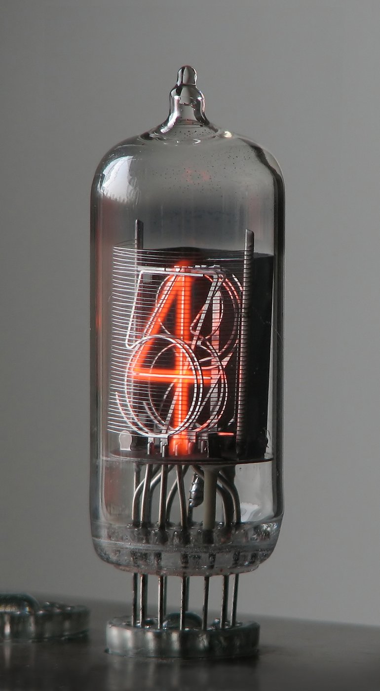
A nixie tube is a beautifully simple display right up until you have to drive it, at which point it asks something no LED ever does: to light the numeral “7” you must take exactly one of ten cathodes and connect it firmly to ground so it can sink a milliamp or two of discharge current, and at the same moment leave the other nine cathodes floating in such a way that none of them strikes — even though every one is sitting a couple of hundred volts away from a hot anode rail that would love to ignite the wrong digit. That is the entire driver problem in one sentence, and it is genuinely a high-voltage problem: a nixie cathode driver is not a logic output, it is a high-voltage open-collector (or open-drain) current sink that must be a dead short to ground when selected and a clean, non-conducting standoff against the anode rail when not. This volume covers the half-dozen ways people have solved it — the classic BCD-to-decimal driver chip, the modern high-voltage shift register, the discrete high-voltage transistor — and the two architectures (direct drive and multiplexing) those parts get wired into. The rail those drivers stand off is the ~170–200 V anode supply of Vol 3; the firmware that decides which digit each second is Vol 5; and the worked ATMega build that ties a real driver chain together is Vol 6. Here we live entirely in the layer between the rail and the tube.
4.1 The driving problem — sink one, stand off nine
Start with the circuit a single tube presents to its driver. The anode connects through a current-limiting anode resistor R_a to the high-voltage rail V_b (Vol 3’s ~170–200 V); the ten numeral cathodes each go to their own driver output. Light a digit and current flows in exactly one loop: V_b → R_a → anode → glow discharge → the selected cathode → that cathode’s driver → ground. The glow discharge holds a nearly constant maintaining voltage V_m across itself once struck (Vol 2) — roughly 120–150 V for the common clock tubes — so the anode node settles to about V_m above the lit cathode, and the anode resistor drops the rest:
   V_b  ──[ R_a ]──┬───────── ANODE (mesh)
  (~180 V)         │            ║  glow discharge (V_m ≈ 140 V when lit)
                   │            ║
        cathode 0 ─○  cathode 1 ─○  ...  cathode 7 ●  ... cathode 9 ─○
        (off)          (off)            (LIT)            (off)
          │              │                │                │
        [drv]          [drv]          [drv ON]           [drv]
        (HV standoff)  (standoff)     (≈0 V, sinks I_k)  (standoff)
          │              │                │                │
         ─┴──────────────┴────────────────┴────────────────┴─  GND
The current is small. Most clock tubes want a cathode current I_k of about 1.5–3 mA — the ZM1210 runs near 2.5 mA, the ubiquitous IN-14 about the same. So the on job is undemanding: be a saturated switch to ground sinking a couple of milliamps with a volt of headroom. The lit cathode sits just above ground (the driver’s saturation voltage), and the anode resistor is sized so the loop delivers I_k — R_a = (V_b − V_m − V_on) / I_k ≈ (180 − 140 − 1) V / 2.5 mA ≈ 16 kΩ, which is why nixie anode resistors land in the 10–22 kΩ range (see Vol 3 for sizing the rail and resistor against tube tolerance).
The hard half is the off job, and it is where all the high-voltage design lives. An off driver presents a high impedance, so its cathode floats — in a tube whose anode is at ~140 V. Through the (non-conducting but not infinite) gas gap and the device’s own leakage, every unlit cathode tries to charge toward the anode potential. The hazard is that an off cathode rises to within a strike voltage of the anode and a second digit ignites, ghosting the display. So the off-state requirement is precise: each off driver must hold its cathode low enough that the anode-to-cathode difference stays well below the tube’s ignition voltage (Vol 2) so the unlit digit stays dark, and do so indefinitely without damage, dissipating only the tiny leakage current it carries while holding off the rail.
The elegant resolution — and the reason a chip rated for far less than 170 V can drive a 170 V tube — is that a well-chosen open-collector output behaves as a soft clamp. As the floating cathode rises, the driver’s output junction enters a gentle reverse avalanche around its rated off-state voltage and quietly holds the cathode there, sinking only microamps. The cathode is pinned tens of volts above ground but a hundred-odd volts below the anode — comfortably under the strike voltage — so the digit stays dark and the IC is unharmed because the clamp current is negligible. That single behavior makes the next three driver families work; each only differs in how high it stands off and how many cathodes it manages per package.

4.2 The classic 74141 / K155ID1 BCD-to-decimal driver
The part that defined nixie driving for a generation is the 74141 — a BCD-to-decimal high-voltage decoder/driver in a single 16-pin package, purpose-built for this job. It takes a 4-bit BCD input (the weighted lines A=1, B=2, C=4, D=8) and decodes it to ten high-voltage open-collector outputs: for each valid digit code, exactly one output is pulled low and the other nine are left high-voltage open, soft-clamped exactly as § 4.1 describes. One chip drives one tube, end to end, with nothing in between but the four logic lines that name the digit. There is no firmware decode, no lookup table, no bit juggling — you present “0101” and pin 5 goes low and the tube shows a 5.
The full truth table, including the blanking codes that make it so useful, is:
Table 1 — The full truth table, including the blanking codes that make it so useful, is
| D | C | B | A | BCD value | Output driven LOW | Display |
|---|---|---|---|---|---|---|
| 0 | 0 | 0 | 0 | 0 | output 0 | 0 |
| 0 | 0 | 0 | 1 | 1 | output 1 | 1 |
| 0 | 0 | 1 | 0 | 2 | output 2 | 2 |
| 0 | 0 | 1 | 1 | 3 | output 3 | 3 |
| 0 | 1 | 0 | 0 | 4 | output 4 | 4 |
| 0 | 1 | 0 | 1 | 5 | output 5 | 5 |
| 0 | 1 | 1 | 0 | 6 | output 6 | 6 |
| 0 | 1 | 1 | 1 | 7 | output 7 | 7 |
| 1 | 0 | 0 | 0 | 8 | output 8 | 8 |
| 1 | 0 | 0 | 1 | 9 | output 9 | 9 |
| 1 | 0 | 1 | 0 | 10 | none | blank |
| 1 | 0 | 1 | 1 | 11 | none | blank |
| 1 | 1 | 0 | 0 | 12 | none | blank |
| 1 | 1 | 0 | 1 | 13 | none | blank |
| 1 | 1 | 1 | 0 | 14 | none | blank |
| 1 | 1 | 1 | 1 | 15 | none | blank |
The last six rows are the gift. Any invalid BCD code (10–15) blanks the whole tube — all ten outputs go open, no cathode is selected, the tube goes dark. That single feature gives leading-zero suppression and the anti-poison cathode-cycling routine a clean mechanism to use (§ 4.6), all without an extra blanking input.
The defining electrical spec is the output’s off-state standoff. The 74141’s outputs hold off the nixie’s off-cathode voltage and soft-clamp there; the datasheet figure is modest — on the order of 55–60 V minimum guaranteed — which is enough because, per § 4.1, the off cathode only needs to be pinned well below the strike voltage, not all the way to ground. The lit output sinks the few-milliamp cathode current saturated to within a volt of ground. The Soviet K155ID1 (К155ИД1) is the pin-for-pin equivalent and the more beloved of the two: plentiful and cheap as NOS, and prized for a notably higher off-state breakdown than the Western 74141, forgiving on tubes with a high maintaining voltage or tall anode rail. Either way the bill is one driver chip and four logic lines per tube.
The 74141/K155ID1 is beloved for its simplicity: it is direct BCD. The microcontroller never has to know which physical pin is the “7”; it emits 7 in binary and the chip does the rest. The cost is also that simplicity — four logic lines per tube adds up (six tubes is 24 lines), the very pin-count pressure the shift-register approach of § 4.3 and the worked build of § 4.8 exist to relieve.

4.3 High-voltage shift registers — the modern path
The modern way to drive a wall of tubes is to stop decoding in hardware and stop spending parallel logic lines, and instead clock a long serial bit-stream into a chain of high-voltage shift registers whose outputs are the cathode drivers. The representative family is Microchip’s (formerly Supertex) HV-series: the HV5622 is a 32-channel serial-to-parallel converter with high-voltage open-drain outputs, and siblings like the HV5530 extend the channel count and voltage rating. Functionally each is a long shift register — data in, a shift clock, a latch/strobe that transfers the shifted bits to the output stage, and a blanking input that forces all outputs off — followed by 32 open-drain transistors that each behave like one cathode driver: pull low when their bit is set, stand off the rail (soft-clamped, § 4.1) when not.
The interface is SPI-flavored and the parts are daisy-chainable: the serial-out of one device feeds the serial-in of the next, so a clock with many tubes runs off one long shift chain on three or four MCU pins (data, clock, latch, blank), regardless of tube count. The channel arithmetic is what makes it dense: one cathode per channel, so a single 32-channel HV5622 directly drives the 30 cathodes of three tubes (two channels spare for decimal points or neon dots). A six-tube clock is two chips and four wires.
The trade against the 74141 is real on both sides:
Table 2 — The trade against the 74141 is real on both sides
| 74141 / K155ID1 (per § 4.2) | HV shift register (HV5622-class) | |
|---|---|---|
| Decode | In hardware — you send 4-bit BCD | In firmware — you send the exact 1-of-10 bit pattern per tube |
| Lines per tube | 4 logic lines | shares one serial chain across all tubes |
| Channels | 10 outputs (1 tube) | 32 outputs (~3 tubes) per package |
| Board density | one chip + 4 traces per tube | one chip per ~3 tubes, 4 traces total |
| Cost | cheap (esp. K155ID1 NOS) | dearer per chip |
| Firmware burden | trivial — emit a number | you build the cathode map and shift 32+ bits per refresh |
The headline win is channel count and board density — fewer chips, far fewer traces, trivial expansion. The headline cost is that the shift register is a dumb 1-of-N driver with no idea what a “digit” is, so the BCD-to-decimal decode now lives in your firmware: you maintain a table mapping each numeral to the one channel that goes low, assemble the whole display’s bit pattern every refresh, and clock it out — a few lines of code you own, where the 74141 hands you the decode for free in silicon.

4.4 Discrete high-voltage transistors
When you want full control, a true high-voltage standoff, or you simply cannot get a driver chip, you build the cathode sink out of discrete high-voltage transistors. The workhorse is the MPSA42, an NPN rated V_CEO ≈ 300 V in a TO-92 — pennies each, and a genuine 300 V standoff that does not lean on the soft-clamp trick at all. Wire it as a common-emitter switch: emitter to ground, collector to the cathode, base through a resistor to the MCU pin. Drive the base high and the transistor saturates, pulling the cathode to near ground and sinking I_k; drive it low and the collector holds off the full anode rail (the unlit cathode floats up to the rail and the 300 V V_CEO sustains it with margin to spare — a cleaner standoff than any 60 V chip). For anode-side (high-side) switching — which multiplexing needs (§ 4.5) — the complement is the MPSA92, a PNP rated about −300 V.
Because the MCU shares the cathode driver’s ground, low-side cathode switching needs no isolation — the emitter sits at 0 V, the same reference as the MCU, so a base resistor is the whole interface. High-side anode switching needs help: the MPSA92’s emitter rides up near the +180 V rail, so its base must be driven relative to that rail — the job of an opto-isolator or level-shift transistor, which lets a ground-referenced 5 V signal switch a base floating 180 V up.
The worked base-resistor calculation makes the cathode sink concrete. Take I_C = 2 mA driven from a 5 V MCU pin. The MPSA42 has modest beta at low current, so design for hard saturation with a forced beta of ~10 — ten times the base current a high-gain transistor would need:
I_B = I_C / β_forced = 2 mA / 10 = 0.2 mA
R_B = (V_pin − V_BE(sat)) / I_B = (5 V − 0.8 V) / 0.2 mA = 4.2 V / 0.0002 A = 21 kΩ
so a standard 22 kΩ base resistor (nearest E12 value) drives 0.2 mA into the base and saturates the transistor solidly at 2 mA collector current, the lit cathode sitting near ground; a 2.5 mA tube with more margin takes 18 kΩ. The discrete path costs two parts per cathode — sixty for a six-tube display — which is why it is reserved for builds that need the true standoff or the control more than the part count, and why the chip approaches dominate finished clocks.

4.5 Direct drive versus multiplexing
There are two ways to wire any of the above into a complete clock, and the choice sets the part count, the brightness budget, and the firmware.
Direct drive gives every cathode its own permanent driver output and lights all tubes continuously. A six-tube clock is six 74141s (or two HV5622s, or sixty discretes), every lit cathode carrying a steady DC milliamp or two. It is the brightest, steadiest, simplest-to-reason-about scheme — and what the worked ATMega build of § 4.8 does. The price is parts: one driver resource per cathode, all populated.
Multiplexing trades parts for time. You light the tubes one at a time in rapid sequence — switch tube 1’s anode on while its cathode drivers paint its digit, then tube 1 off and tube 2 on, round the display — so a single shared set of ten cathode drivers serves all tubes. The like-numbered cathodes of every tube are bused together (all the “0” cathodes to one driver, all the “1”s to the next), and N high-side anode switches (the MPSA92 / HV P-MOSFET of § 4.4) steer the discharge to whichever tube is currently “on.” One 74141 plus six anode switches can run a six-tube clock — a large saving in cathode drivers.
The catch is the brightness math. With N tubes each is lit only 1/N of the time, so its duty cycle is 1/N and its average current is the peak current scaled by that duty:
I_avg = I_peak × duty = I_peak / N
To make a multiplexed tube look as bright as a direct-driven one — i.e. to hold I_avg at the same ~2 mA — the peak current must rise by the factor N:
I_peak = I_avg × N = 2 mA × 6 = 12 mA
so a six-digit multiplexed clock fires each tube at ~12 mA in 1/6-duty bursts to net the same 2 mA average glow. Both the tube and the shared cathode drivers must tolerate that peak, and the anode resistor is re-sized for it. The other constraint is refresh rate: the display must cycle fast enough that the eye fuses the bursts into steady light. Keep the per-tube refresh at ≥ ~60–100 Hz — for six tubes that means the anode-switch sequence runs at 6 × 100 Hz = 600 Hz, each tube getting a ~1.67 ms slot in a 10 ms frame. Slower and the display visibly flickers; the gas’s finite ionization delay (the tens of microseconds a cold cathode needs to strike each time it is re-lit) also nibbles the start of every slot, wasting brightness and flooring how fast you can usefully multiplex. The honest trade: multiplexing slashes the cathode-driver count and is the natural partner of the shift-register and discrete approaches, at the cost of higher peak currents, an anode-switching stage, tighter timing, and a little less brightness than direct drive. The ATMega build of § 4.8 exists in both flavors — direct-drive and multiplexed — so the trade can be seen side by side (Vol 6).

4.6 Blanking, leading-zero suppression, and anti-poison control
The driver layer is also where three housekeeping behaviors get implemented, all of them just the absence of a lit cathode applied cleverly. Blanking is the primitive: make a whole tube dark on command. With a 74141 you blank by driving its BCD inputs to any invalid code 10–15 (§ 4.2); with a shift register you blank by clearing that tube’s ten bits (or asserting the chip’s blank input); with discretes you simply drive no base. Every driver family gives you a clean “show nothing” state, and the higher layers spend it three ways.
Leading-zero suppression is the cosmetic use: a clock should read ” 9:25”, not “09:25”, so the tens-of-hours tube blanks when its digit would be a leading zero. The tidy implementation is a ripple-blank: a digit blanks for a leading zero only if every more-significant digit is also blanked, so the suppression ripples in from the left and stops at the first non-zero digit.
Anti-poison cathode cycling is the maintenance use — the driver-layer realization of the cathode-poisoning countermeasure of Vol 2. Cathodes left unlit for long periods accumulate sputtered metal and grow reluctant to strike; the cure is to periodically exercise every cathode of every tube through all ten numerals so the glow cleans each. The driver layer runs this as a routine — at a quiet hour, or as a brief “slot-machine” flourish — by sequencing the BCD codes 0→9 rapidly on each tube (74141), or walking the lit bit through all ten channels (shift register). It is the same one-low-nine-off hardware; only the sequence of which cathode is low changes, and that sequence is the firmware’s business (Vol 5).

4.7 Dimming and transition effects
Because the driver layer controls when current flows, not just whether, it is also where brightness control and the signature nixie transition effects are produced — all by pulse-width modulation of the same on/off states.
Global dimming is cleanest on the anode side. PWM the anode switch (or the HV rail feeding it) at a frequency above flicker — several hundred Hz to a few kHz — and the average current through every lit tube falls with the duty cycle, dimming the whole display uniformly without touching the cathode pattern. This is the same high-side switch the multiplexing of § 4.5 already uses, so on a multiplexed clock dimming is nearly free (shorten each tube’s lit slot); a direct-drive clock adds one anode-PWM switch for the same global dimmer (a night/day schedule). Cathode-side PWM works but dims one tube at a time and fights the multiplex timing, so anode PWM is the usual choice for global brightness.
Crossfade transitions are the effect people build nixie clocks for. When a digit changes from 5 to 6, instead of snapping you rapidly alternate the outgoing cathode (5) and the incoming cathode (6) with a duty cycle that slides from all-5 to all-6 over a few tens of milliseconds — the 5 fades out as the 6 fades in. The slot-machine variant scrolls through the intermediate numerals so the digit appears to spin into place. Both are pure driver-layer tricks needing a fast-switching driver and a firmware PWM loop — natural on shift-register and discrete drivers, and doable on a 74141 by time-slicing its BCD inputs between the two codes. The one physical limit is the gas: the discharge’s de-ionization time means a cathode cannot be switched infinitely fast, which is why crossfades run over tens of milliseconds, not microseconds.

4.8 The ATMega Cool Nixie Clock’s driver chain (worked example)
The hub’s worked build ties this volume’s theory into a real data path, and it is a textbook
example of the 74141 + shift-register marriage that gets the best of both worlds: the
74141’s free hardware decode and a shift register’s low pin count. The display board’s
schematic (zm1210-display-atm-7.sch) confirms the topology directly — 74141N BCD
drivers, one per ZM1210 tube, sinking the cathodes exactly as § 4.2 describes. What feeds
those 74141s is the clever part: the ATMega MCU does not wire 24 BCD lines out to six
chips. Instead it shifts the BCD data serially into a chain of 74HC595 shift registers,
whose parallel outputs drive the 74141 BCD inputs.
The 74HC595 is an 8-bit serial-in / parallel-out shift register with an output latch and the standard pinout the build relies on:
- SER — serial data in (one bit per clock).
- SRCLK — shift-register clock; each rising edge shifts SER one position along the chain.
- RCLK — storage-register (latch) clock; a rising edge transfers the eight shifted bits to the output pins all at once, so the outputs change cleanly only when a whole frame is loaded.
- OE (output enable, active low) — gates the parallel outputs on/off, handy for blanking or PWM dimming.
- SRCLR (shift-register clear, active low) — zeroes the shift register.
- QH′ — the serial-out tap that daisy-chains one 595 into the SER of the next.
The data path each update is therefore: the ATMega assembles the six digits as BCD, then bit-bangs (or SPIs) the bits out on SER, clocking each with SRCLK, walking the word down the daisy chain through the QH′→SER cascade; with the last bit in place it pulses RCLK once to latch every 595’s outputs at once; those outputs present stable BCD to the six 74141N decoders, which each pull one ZM1210 cathode to ground and stand off the rail on the other nine. Six tubes × 4 BCD bits = 24 bits, so the chain is three cascaded 74HC595s (8 bits each) driving the six 74141s — and the ATMega has spent just three pins (SER, SRCLK, RCLK) to control the whole display. Critically, the 74HC595s are ordinary 5 V logic and never touch high voltage — they only set the BCD inputs of the 74141s; the 74141 is the sole high-voltage part in the chain, confining the ~170 V to the driver chips and tubes (the rail itself is Vol 3’s).
The folder also holds a multiplexed variant (2D3 Nixie clock Schematic (Multiplexed).pdf)
applying § 4.5: rather than a 74141 per tube lit continuously, it shares cathode drivers and
sequences the tube anodes, trading driver count for higher peak current. The two schematics
are the direct-drive and multiplex options of this volume made concrete. The complete build —
BOM, PCB, firmware (nix-in-17), bring-up — is Vol 6; the driver story here is simply that an
ATMega, three shift registers, six BCD drivers, and six tubes is all it takes to put six
glowing numerals in the air.

4.9 References (Vol 4)
- ATMega Based Cool Nixie Clock — display schematic
zm1210-display-atm-7.sch(confirms 74141N BCD drivers, one per ZM1210/12 tube), the multiplexed variant2D3 Nixie clock Schematic (Multiplexed).pdf, the74HC_HCT595.pdfshift-register datasheet (SER/SRCLK/RCLK/OE/SRCLR/QH′ pin functions and daisy-chaining),ATMegaManual.pdf, thenix-in-17firmware, andnixiepcb.zipPCB gerbers. Held in02-inputs/ATMega Based Cool Nixie Clock/. - Texas Instruments / Fairchild SN74141 BCD-to-decimal decoder/driver datasheet — truth table, the 10–15 blanking codes, and the open-collector off-state rating.
- Soviet К155ИД1 (K155ID1) datasheet — the pin-compatible 74141 equivalent with the more robust off-state breakdown prized for nixie work.
- Microchip (formerly Supertex) HV5622 (32-channel) and HV5530 HV serial-to-parallel open-drain shift-register datasheets — channel count, data/clock/latch/blank interface, daisy-chaining, HV output ratings.
- MPSA42 (NPN, V_CEO ≈ 300 V) and MPSA92 (PNP, ≈ −300 V) transistor datasheets — the discrete cathode-sink and anode-switch parts.
- Telefunken/Philips ZM1210 and Soviet IN-14 tube data — maintaining/strike voltages and cathode current behind the anode-resistor figures.
- Sibling volumes: Vol 2 (glow-discharge physics, poisoning), Vol 3 (the ~170–200 V supply and anode-resistor sizing), Vol 5 (firmware), Vol 6 (the full ATMega Cool Nixie Clock build).
Comments (0)