Relay Nixie Clock · Volume 3
Building It
My 54-relay board, the details the designer's documents leave out, a staged assembly order that tests each block before the next, and the build log
This volume is the build. It starts with the board I have, collects everything the designer’s datasheet and schematic leave out or get wrong, and then sets out an assembly order that brings the clock up one block at a time, each tested before the next goes in. It ends with the build log, which grows as the build does.
The nixie supply is part of this build, but its review and its part changes are in Volume 2, and its bring-up procedure (§2.6) is the first stage below.
3.1 My board
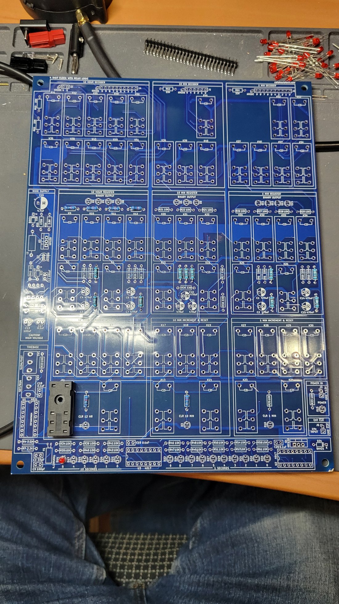
The board is silkscreened “4 DIGIT CLOCK WITH RELAY LOGIC” and “catahoulatech.com”, and it is the later, 54-relay revision. The designer’s datasheet (dated 2021-08-09) still shows the earlier layout, with three relay positions across the top of the 1-minute decoder: K46, K52 and K53. My board has only K52 and K53 there. The designer’s project page explains the change: “The newer revision of the board only requires 54 relays as a relay in the 1 min decoder was not necessary.”1
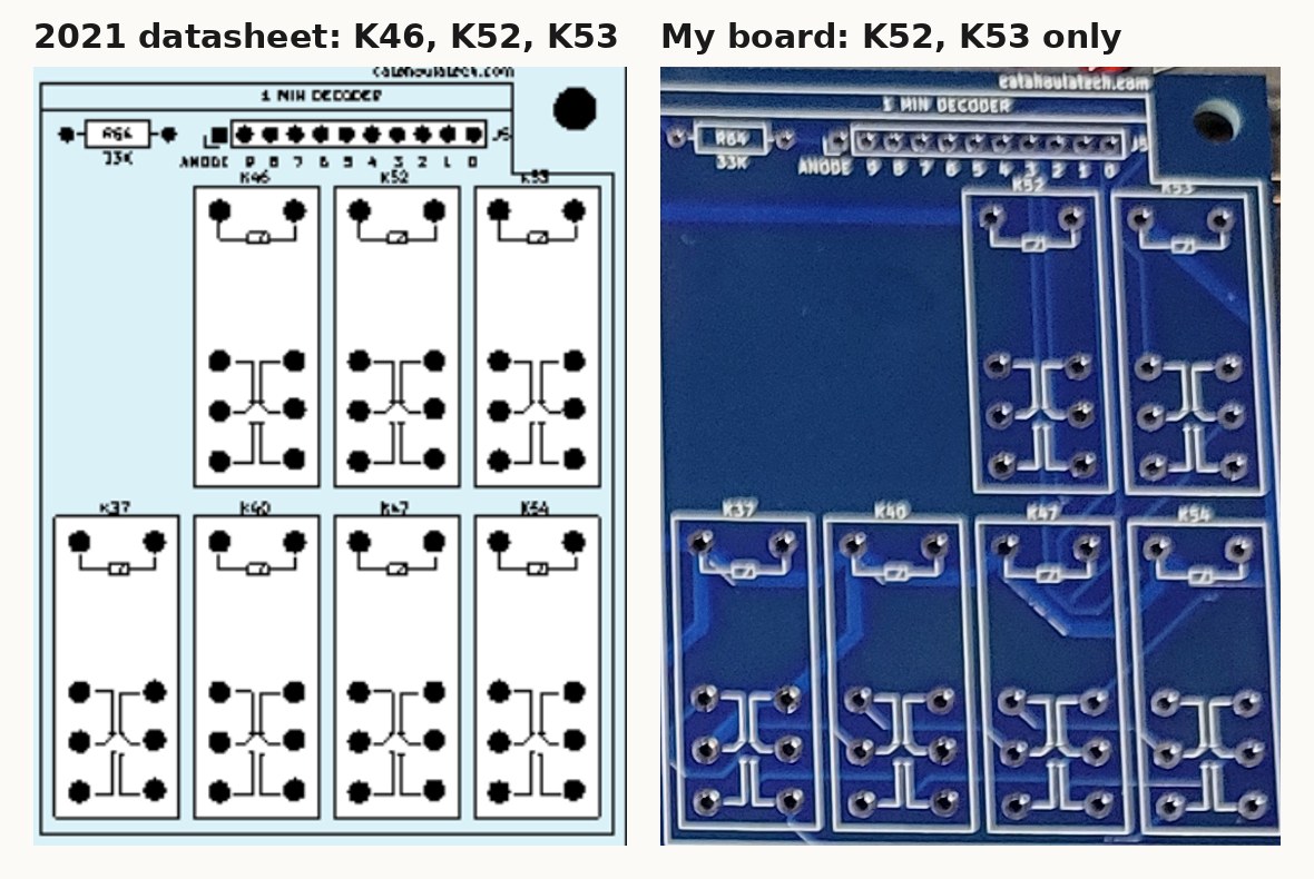
So the datasheet’s “K1–K55” means 54 relays on this board: every number from K1 to K55 except K46. The schematic (2021-08-10) already reflects the 54-relay logic: its 1-minute decoder has six relays and no K46 (Volume 1, Figure 1.6). The designer’s own photos and placement drawing are of the older board, which is where an extra relay in the upper right corner comes from.
3.2 What the designer’s documents leave out
These are the points that are missing, wrong, or easy to misread in the datasheet, BOM and schematic, checked against each other and against my board.
Table 1 — 3.2 What the designer's documents leave out
| # | Item | What the documents say | What is actually needed |
|---|---|---|---|
| 1 | Relay count | BOM: K1–K55, G2R-2-12VDC | 54 on this board; there is no K46 (§3.1) |
| 2 | R11 | Not in the BOM | 10 Ω, the sampling resistor for hour bit D1 (K4). On the schematic and silkscreen. |
| 3 | R33 | Not in the BOM | 100 Ω, the gate resistor for Q1 (/CLK driver). On the schematic and silkscreen. |
| 4 | C16 | Not in the BOM | 4.7 µF, 250 V or higher: the HV reservoir (Volume 2) |
| 5 | R56 | 3.8 kΩ | Not a standard value; replace per Volume 2 (3.40 kΩ for CD72s) |
| 6 | Voltage ratings | Only “16V” on the low-voltage capacitors | C16 ≥ 250 V; everything else is on the 12 V rail |
| 7 | Tube wiring | Header pin lists, no tube type or pinout | Header maps in §3.5; the 1-hour header runs in a different order from the others |
| 8 | Leading zero | Not mentioned | The 10-hour tube shows “0” for hours 1–9 unless its “0” pin is left unwired (§3.5) |
| 9 | EXT CLK | ”Active low external 1Hz reference” | Wired to the minute clock line itself: it advances one minute per pulse (Volume 4) |
| 10 | Coil suppression | Only D34, on the /CLK line | No flyback diodes on the other 48 coils; their contacts absorb the inductive kick. As designed, and the board has no pads for more. |
Items 2–4 matter most. A BOM-only parts order leaves out three components, and two of them are in places where the clock still powers up and half-works: without R11, one hour bit never samples its next value, and without C16 the HV supply has no output capacitor at all.
From the photo, the R11 position on my board is still empty while the other nine 10 Ω resistors are in. That fits a parts kit built from the BOM, and it is on the list for the next session.
3.3 Parts
Table 2 — 3.3 Parts
| Group | Parts | Notes |
|---|---|---|
| Relays | 54 × Omron G2R-2-12VDC (DPDT, 12 V coil, 275 Ω) | The designer links a TME listing. Use the plain DC part; the “-SD” diode variant releases more slowly, and the register timing in Volume 1 assumes the plain coil. |
| Sampling capacitors | 10 × 470 µF 16 V, 5 mm, 2.5 mm pitch | C1, C2, C4–C8, C10, C11, C14, C15. 105 °C parts are worth the small premium; these set the register timing margins (Volume 1, §1.3). |
| Resistors | 10 Ω × 11 (incl. R11), 330 Ω × 11, 10 kΩ × 31, 33 kΩ × 4 (anodes, see Volume 2), plus R4, R7, R33, R43–R45, R55, R56 | 1/4 W. R43/R44 (BOM 0.5 Ω, hard to find at 1/4 W): I am fitting one 0.51 Ω and one 0.47 Ω (5%; every other resistor is 1%), 0.245 Ω in parallel, for a current limit of about 1.23 A (0.97–1.50 A worst case). |
| CMOS | CD4521, 2 × CD4017, MC34063AP | Sockets recommended for all four. |
| Semiconductors | 2 × STF8N65M5 for both Q1 and Q3 (Q3 per Volume 2; the IRF740 is obsolete, and one part type serves both — at Q1 it sinks the six sampling coils, about 0.26 A, fully on from the 12 V CMOS gate drive), 2N3906, 1N4148, 2 × UF4004 at D28 and D34, replacing both BAV21s (check the 0.8 mm leads fit) | |
| LEDs | 31 × 3 mm | Seconds (16), register bits (11), CLR indicators (3), power (1). |
| Crystal | 4.194304 MHz | |
| Other | L1 Würth 744743101 (100 µH, I_sat 2.1 A, radial: mounting in Volume 2, §2.5), 2 SPDT slide switches, 0.1 in headers J1–J6 | |
| Tubes | 4 × IN-14 new-old-stock (my choice; the designer used CD72s2) | Off-board, wired to the headers. Anode resistors and R56 per Volume 2 §2.5 (18 kΩ, 3.30 kΩ). |
| Tube sockets | 4 × IN-14 PCB socket, 13 gold machined-pin contacts | §3.5. Sold without cable. |
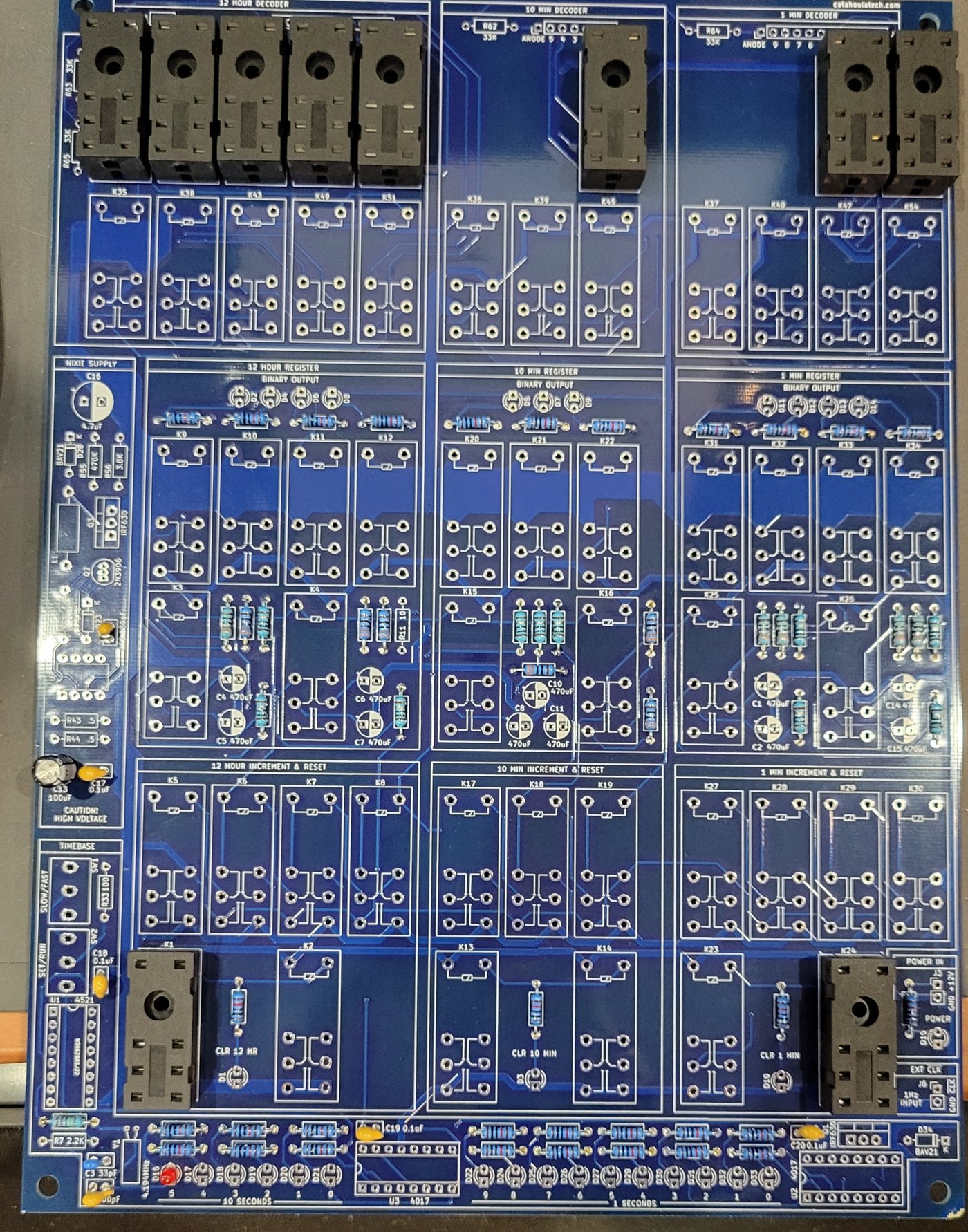
Relay sockets. I test-fitted a relay socket at K1 (Figure 3.1). Sockets make a relay swappable, which is attractive with 54 of them, at the cost of 54 more parts and a taller board. Check that the socket’s pins match the G2R-2 footprint and that a relay seats firmly in it before committing to one.
I am socketing all 54 relays, so any relay that wears out or sticks can be pulled and swapped without desoldering eight pins. The sockets fit the G2R-2 footprint perfectly (Figure 3.4). Because the finished clock will hang on a wall, every relay also gets a wire retaining bail, so none can work loose from its socket under its own weight or a knock.
3.4 Assembly order: one block at a time
The temptation with a board like this is to stuff all 54 relays and switch on. Don’t. Each stage below adds one block and tests it before the next. Every later stage relies on the earlier ones being known-good, and a fault found in a ten-part block is far easier to find than one hidden among four hundred.
General points throughout: LED flats and the short lead are the cathode; electrolytic stripes are negative; fit the low parts (resistors, diodes) before the tall ones (capacitors, relays) in each block; and power every test from a current-limited bench supply, not a wall adapter.
3.4.1 Stage 1 — Power and the nixie supply
Fit POWER IN, the power LED (D15) and its resistor, and the NIXIE SUPPLY strip with the Volume 2 changes. Run the Volume 2 §2.6 bring-up in full: voltage, bleed-down time, one tube under load, half an hour of running. Then remove the test tube and bleed C16 before carrying on. The HV stays live on the board through every later stage.
3.4.2 Stage 2 — Timebase and seconds
Fit U1, Y1, C3, C9, R4, R7, U2, U3 (in sockets), the seconds LEDs (D16–D21 for the tens, D22 and D24–D33 for the units) with their 10 kΩ resistors, SW1, SW2, R33, Q1, D34, J6 and the decoupling capacitors C18–C20 (C17 went in with the nixie supply).
Tests:
- The units LEDs step once a second and the tens LEDs once every ten seconds, 0 to 5.
- /CLK. With no relays fitted, nothing pulls /CLK up, so temporarily connect a 1 kΩ resistor from /CLK (J6 pin 1) to +12 V and watch it with a meter or scope. In RUN it should sit at 12 V and drop to near 0 V for ten seconds each time the tens LEDs show 0. In SET it should follow a 1 Hz (SLOW) or 8 Hz (FAST) square wave. Remove the resistor afterwards.
3.4.3 Stage 3 — The 1-minute digit
Fit the whole 1-minute chain: register (K25, K26, K31–K34, C1, C2, C14, C15, R1, R2, R52, R53, R5, R6, R59, R60, the binary LEDs D11–D14 with R26–R29), increment and reset (K23, K24, K27–K30, the CLR 1 MIN LED D10 and R25) and decoder (K37, K40, K47, K52, K53, K54).
Test with SW2 on SET and SW1 on SLOW: the four binary LEDs must count 0000 to 1001 and wrap to 0000, one step per second, and the CLR 1 MIN LED must light while the count is 1001 (9). Then switch to RUN and confirm the count advances once a minute, at :00. With an ohmmeter (HV off and bled), check that J5 grounds exactly one cathode pin for each count (§3.5).
3.4.4 Stage 4 — The 10-minute digit
Fit the 10-minute register (K15, K16, K20–K22, C8, C10, C11, R30–R32, R36–R38, the binary LEDs D5, D7, D9 with R21, R22, R24), increment and reset (K13, K14, K17–K19, CLR 10 MIN LED D3) and decoder (K36, K39, K44, K45). In SET/FAST, the 10-minute LEDs must step each time the minutes wrap and roll 101 (5) → 000 after the 59th minute, with CLR 10 MIN lighting only during minute 59 of each hour.
3.4.5 Stage 5 — The hours
Fit the hour register (K3, K4, K9–K12, C4–C7, R8, R9, R11, R13, R17–R20, binary LEDs D2, D4, D6, D8 with R10, R12, R14, R16), increment and reset (K1, K2, K5–K8, CLR 12 HR LED D1 with R3) and decoder (K35, K38, K41, K42, K43, K48–K51, K55). In SET/FAST, run a full twelve hours: the hour register must count 0000 to 1011 and return to 0000 exactly at 12:59 → 1:00, with CLR 12 HR lighting only at 12:59.
3.4.6 Stage 6 — Tubes
Mount the four IN-14 sockets, wire them to J1, J2, J4 and J5 (§3.5), and fit the 18 kΩ anode resistors chosen in Volume 2. With HV off and bled, check every socket contact against its header pin with an ohmmeter before any tube goes in. Then seat the tubes and power up. Check every digit of every tube in SET/FAST, and watch the minute digit across several real minute changes for any digit that is slow to strike (Volume 2, finding 1).
3.5 Wiring the tubes
Each header carries the tube’s anode on pin 1 (fed from +HV through its anode resistor on the board) and the cathodes on the remaining pins, which the decoder pulls to ground. The pin order, from the schematic:3
Table 3 — 3.5 Wiring the tubes
| Header | Tube | Pin 1 | Then pins 2, 3, 4 … in order |
|---|---|---|---|
| J5 | 1-minute | anode (R64) | 9, 8, 7, 6, 5, 4, 3, 2, 1, 0 |
| J1 | 10-minute | anode (R62) | 5, 4, 3, 2, 1, 0 |
| J4 | 1-hour | anode (R65) | 0, 9, 8, 7, 6, 5, 4, 3, 2, 1 |
| J2 | 10-hour | anode (R63) | 1, 0 |
Note J4: the 1-hour header starts at 0 and then runs 9 down to 1, unlike J5, which runs 9 down to 0. Wiring J4 in J5’s order shifts every hour by one.
Blanking the leading zero. J2 pin 3 is the 10-hour tube’s “0”. Leave it unconnected and the tube is simply dark for hours 1 to 9 and shows “1” for 10, 11 and 12. A nixie with no cathode grounded draws no current; its anode just sits at HV through the resistor, which is harmless. This is a wiring choice, not a board change, and it is easy to reverse.
3.5.1 The IN-14 sockets
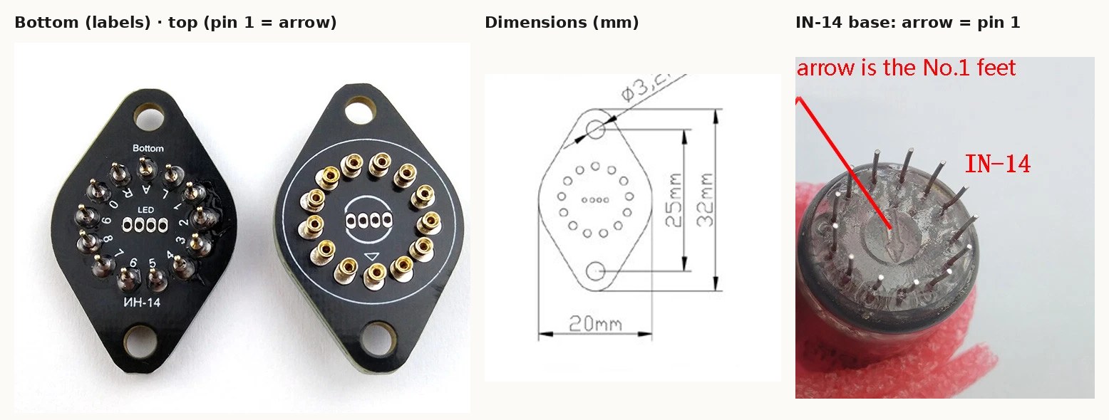
I am mounting the tubes in small IN-14 PCB sockets rather than soldering to their leads, so a tube can be swapped without a soldering iron. Each socket is a diamond-shaped board, 32 × 20 mm, with 13 gold machined-pin contacts in a ring and two Ø3.2 mm mounting holes on 25 mm centres, so M3 screws mount it to a panel or standoffs. The contacts take tube leads from 0.3 to 0.7 mm. The sockets come without cable.
Wire by the labels. The solder side labels every contact: A for the anode, L and R for the decimal points, and 0–9 for the digits. (The listing’s annotated photo calls two different pins “Right decimal point”; the silkscreen’s L and R are correct.) With the labels, there is no need to work out the IN-14’s base pinout; the socket has done it. Matched to the RL1200 headers:
Table 4 — Wire by the labels. The solder side labels every contact: A for the anode, L and R for the decimal points, and 0–9 for the digits. (The listing's annotated photo calls two different pins "Right decimal point"; the silkscreen's L and R are correct.) With the labels, there is no need to work out the IN-14's base pinout; the socket has done it. Matched to the RL1200 headers
| Header | Tube | Pin 1 | Pins 2, 3, 4 … | Socket contacts left empty |
|---|---|---|---|---|
| J5 | 1-minute | → A | → 9, 8, 7, 6, 5, 4, 3, 2, 1, 0 | L, R |
| J1 | 10-minute | → A | → 5, 4, 3, 2, 1, 0 | 6–9, L, R |
| J4 | 1-hour | → A | → 0, 9, 8, 7, 6, 5, 4, 3, 2, 1 | L, R |
| J2 | 10-hour | → A | → 1, 0 | 2–9, L, R |
That is 32 wires in all. I am keeping the leading zero, so the 10-hour “0” is wired and the clock reads 09:41, not 9:41; leaving that one wire off would blank it. The RL1200 has no decimal-point drive, so L and R stay empty on every socket.
The centre pads are for a backlight. The four pads marked LED in the middle of each socket are for an RGB LED under the tube. The RL1200 has nothing to drive them, so they stay empty.
Fitting the tubes:
- Orientation. The ▽ on the tube side of the socket marks pin 1, and the IN-14 has an arrow moulded into the glass of its base pointing at pin 1. Line the two up.
- Trim the leads. The seller specifies leaving 4–10 mm of lead below the base. Trim all of a tube’s leads to the same length so they enter the contacts together.
- Clean them. New-old-stock leads are often dull with oxide. A light rub with fine abrasive gives the contacts something clean to grip.
- Push straight. Seat a tube by pressing it straight in, not by rocking it. The glass-to-lead seal at the base is the fragile part of a nixie.
Wiring and safety. Solder the wires to the contact tails on the solder side. Use wire insulated for at least 300 V: every contact carries up to the full HV whenever its digit is off, not just the anode. Give each tube’s bundle some strain relief so the solder joints do not carry the cable’s weight, and cover the backs of the sockets in the finished clock (Volume 4, §4.7).
3.6 Safety during the build
The NIXIE SUPPLY strip makes over 150 V DC, and from Stage 1 onward it is live whenever the board is powered, including while you are working on the relay sections next to it. Habits for this build:
- Power off, wait ten seconds, and measure +HV before touching anything. The divider bleeds C16 in a few seconds; confirm it every time.
- Probe with one hand. Clip leads on with the power off.
- A clear cover over the NIXIE SUPPLY strip and the tube wiring for the finished clock (Volume 4).
- The hub’s safety baseline and the Nixie overview’s safety volume apply in full.
3.7 Buy instead of build
Catahoula Technologies sells the RL1200 board, and the relay-logic modules the design grew out of, through its store linked from the designer’s project page.1 Availability and price are not recorded here: check the store. There is no finished, ready-to-hang version of this clock; the board is the kit.
3.8 Build log
- 2026-10-28. Board in hand: the 54-relay revision (Figure 3.2). From the day’s photo: the 10 Ω sampling resistors are in except R11 (missing from the BOM), along with the hour register’s LED resistors (R10, R12, R14, R16), the CLR indicator resistors and the first seconds LED (D16), with a relay socket test-fitted at K1. The 470 µF capacitors and all relays are still to go in. Nixie supply reviewed (Volume 2) before any of its parts are fitted.
- 2026-10-28 (later). Tubes chosen: new-old-stock IN-14s, ordered with four IN-14 PCB sockets (§3.5). That fixes the HV values: R56 = 3.30 kΩ, 18 kΩ anode resistors, a 400 V+ MOSFET for Q3 (STF8N65M5, since the IRF740 proved obsolete) (Volume 2, §2.5).
- 2026-10-28 (later still). Decided: keep the leading zero (J2 pin 3 wired), socket all 54 relays, use STF8N65M5 MOSFETs for both Q1 and Q3, and use a Würth 744743101 for L1, standing upright with one lead sleeved across to the second hole. Power-supply part changes under review (Volume 2, §2.5).
- 2026-10-28 (later still). C13 fitted: 100 µF 25 V. C16 ordered at 350 V. D28 and D34 both to be UF4004. That completes the power-supply decisions (Volume 2, §2.5).
- 2026-10-28, 13:23. Most of the resistors are in: the register 10 Ω, 330 Ω and LED resistors, all the seconds-LED and CLR-indicator resistors, and R4, plus C3, C9, C12, C17, C18–C20 and C13 (25 V). Ten relay sockets test-fitted and they fit perfectly; retaining bails on hand for every relay. Still empty: R11 (I ran out of 10 Ω resistors; more on order), R7 and R33, and R43/R44 (on order).
- 2026-10-28 (end of day). Parts complete apart from C16: all the 1% resistors, the 54 relays and their sockets, and the IC sockets are on hand, and everything else has been ordered. The 350 V C16 is the one part still to arrive.
3.9 References (Vol 3)
Footnotes
-
Jon Stanley, “Relay Logic Projects”, electronixandmore.com, https://www.electronixandmore.com/projects/relaylogic/index.html (checked 2026-10-28). ↩ ↩2
-
Jon Stanley, project index, https://www.electronixandmore.com/projects: “A 4-digit nixie clock using CD72 nixies and relay counting logic on a PCB”. ↩
-
Catahoula Technologies, 12-hour 4-digit relay clock schematic, 2021-08-10; datasheet with BOM and placement, 2021-08-09. Both held in this clock’s
02-inputs/Designer - Catahoula RL1200/. ↩
Comments (0)