Relay Nixie Clock · Volume 2
The Nixie Power Supply
A review of the RL1200's MC34063 boost converter: what is sound, what is under-rated, and the part changes it needs before it powers a tube
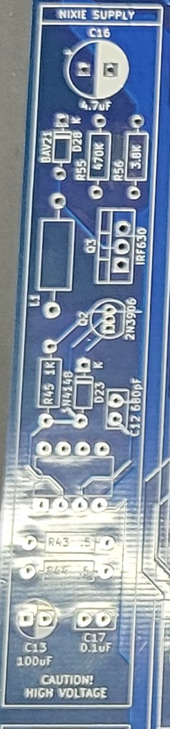
The RL1200 makes its anode voltage on the board, from the same 12 V that runs the relays, with a small boost converter in the left-hand strip marked “NIXIE SUPPLY / CAUTION! HIGH VOLTAGE”. It deserves a review before any of its parts go in: it is the one part of this clock that can hurt someone, and the one part the designer documents least.
The short version: the circuit topology is sound and well proven, but as specified it runs the tubes below their rating, and three of its parts are under-rated for the current the circuit actually pushes. None of that needs a redesign. It needs one resistor value, four anode resistors, and three better parts, all of which fit the existing footprints (one should be checked for lead diameter). The rest of this volume shows the working.
High voltage first. This supply makes more than 150 V DC from a 4.7 µF capacitor. Read the hub’s safety baseline and the Nixie overview’s safety volume before working on it, and follow the bring-up order in §2.6.
2.1 What the tubes need
The designer built his clock with CD72 tubes.1 The CD72 is a small Matsushita end-view nixie with 12 mm digits, specified for a 170 V minimum supply, a 140 V typical maintaining voltage, and a 1.5 mA typical cathode current,2 with 1 mA minimum and 2 mA maximum quoted elsewhere.3
Two numbers matter. The supply must be high enough for a cathode to strike, that is, to start glowing from cold. The current, set by the anode resistor, must be high enough for the glow to cover the whole digit. On this clock, every digit change is a fresh strike: when a decoder relay moves, the old cathode is disconnected and the new one must light from nothing. A supply too close to the strike voltage shows up as a digit that blanks, or lights late, after the minute changes.
The RL1200 wires its tubes off-board through 0.1 inch headers, so any tube can be used. For comparison, the Russian IN-14 is rated for a firing voltage up to 170 V and a working current up to 2.5 mA,4 and the IN-12 for 2.5 to 3.5 mA.5 Both want at least as much as the CD72.
2.2 How the circuit works
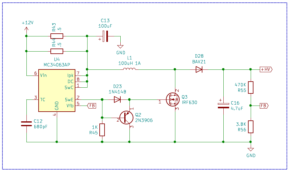
This is the classic MC34063 nixie boost converter with an external high-voltage MOSFET, the same arrangement many nixie kits use.6
- U4, MC34063AP, is a 1980s switching-regulator chip with an oscillator, a comparator against a 1.25 V reference, a current-limit sense input and a Darlington output switch.7
- The switch is not the chip’s own transistor, which cannot stand off 150 V. U4’s output (SwE, pin 2) drives Q3, an IRF630 MOSFET, through D23 as an emitter follower. When U4’s switch turns off, R45 pulls the base of Q2 (2N3906) low and Q2 dumps the MOSFET’s gate charge quickly. With pin 8 tied to the collector side, the gate reaches roughly 12 V − 0.3 V (sense) − ~1 V (Darlington) − 0.6 V (D23) ≈ 10 V, enough to switch the IRF630 fully on.
- L1 (100 µH) charges from 12 V while Q3 is on. When Q3 turns off, the inductor’s voltage flies up and D28 (BAV21) delivers the energy into C16 (4.7 µF), the HV reservoir.
- R55 (470 kΩ) and R56 (3.8 kΩ) divide the output down to U4’s 1.25 V comparator. The chip skips switching cycles whenever the divided voltage is above 1.25 V. The divider also bleeds C16 when power is removed.
- R43 ∥ R44 (two 0.5 Ω, so 0.25 Ω) sit in the 12 V feed. When the voltage across them reaches the chip’s current-limit threshold, U4 ends the on-time.
- C12 (680 pF) sets the oscillator. C13 (100 µF) decouples the 12 V input.
2.3 The operating point as designed
Output voltage. The MC34063 regulates the divider’s midpoint to 1.25 V (1.225 to 1.275 V across parts):7
V_HV = 1.25 V × (1 + R55 / R56) = 1.25 × (1 + 470 / 3.8) = 155.9 V
spread from the reference alone: 152.7 V to 159.0 V
Tube current. With 33 kΩ anode resistors (R62–R65) and a CD72 maintaining about 140 V:
I_tube = (155.9 V − 140 V) / 33 kΩ = 0.48 mA
         (0.63 mA if the tube maintains at 135 V, 0.33 mA at 145 V)
Peak switch current. The current limit is set by the sense resistance:
I_pk = V_sense / R_sense = 0.30 V / 0.25 Ω = 1.2 A (1.0 A to 1.4 A over the 0.25–0.35 V spread)Does the circuit actually reach that limit, or does the oscillator end each on-time first? The MC34063’s timing capacitor relation (C_T = 4.0 × 10⁻⁵ × t_on) gives a maximum on-time with 680 pF of about 17 µs.7 In that time 12 V across 100 µH would ramp the inductor to 12 V × 17 µs / 100 µH ≈ 2.0 A. The limit trips first, so every switching cycle that runs ends at about 1.2 A. The chip regulates by skipping whole cycles, not by shortening them. The inductor, MOSFET and diode see that full peak on every cycle, however lightly the tubes are loaded.
2.4 Findings
Ranked by consequence:
Table 1 — Ranked by consequence
| # | Finding | As designed | What it should be |
|---|---|---|---|
| 1 | Supply below the CD72’s minimum | 156 V (153–159 V) | ≥ 170 V for a reliable strike |
| 2 | Tube current a third of typical | 0.48 mA per tube | ~1.5 mA (CD72); ~2–2.5 mA (IN-12/IN-14) |
| 3 | D28 over its peak rating | BAV21: 625 mA repetitive peak,8 sees 1.0–1.4 A | A 1 A fast-recovery diode |
| 4 | L1 at or past its rating | ”100 µH 1 A”, sees 1.0–1.4 A peaks | Saturation current ≥ 1.5 A |
| 5 | Q3 margin thin once the voltage is raised | IRF630, 200 V | 500–650 V part with low gate charge (STF8N65M5) |
| 6 | C16 missing from the BOM | Silkscreen says 4.7 µF; no voltage given | 4.7 µF, 250 V or higher, 105 °C |
| 7 | R56 is not a standard value | 3.8 kΩ (3.83 k is E96; 3.9 k is E24 → 152 V) | Replaced anyway by finding 1 |
| 8 | Input capacitor rating tight | C13 100 µF 16 V on a 12 V rail | 25 V |
1 and 2: the tubes are under-driven. The designer’s own clock clearly works,1 so this is a margin problem, not a broken design. But at 156 V a CD72 is being asked to strike from 14 V below its rated minimum supply, and at 0.48 mA it is running at half its minimum current. Expect a dim glow that may not cover the whole numeral, and, on some tubes, digits that fail to strike after a decoder relay changes them. Tube-to-tube spread decides whether a given set copes. On IN-12 or IN-14 tubes the shortfall is worse.
3: the BAV21 is the weak part. Every cycle starts the diode’s conduction at the inductor’s peak current, 1.0–1.4 A, and the BAV21 is rated for 625 mA repetitive peak forward current.8 It is also end-of-life at Nexperia.8 It may survive for a long time at a low duty cycle, but it is operating outside its rating on every pulse.
4: the inductor. A “1 A” rating on a small axial inductor is usually a thermal (RMS) rating, and its saturation current can be lower. Peaks of 1.0–1.4 A put it at or past that point. A saturating inductor makes the current ramp steeply at the end of the on-time, which raises the stress on the MOSFET and diode further.
5: the MOSFET. The IRF630 is a 200 V part. At 156 V there is some headroom; at the 170–180 V the tubes want, plus switching overshoot, there is not enough. The obvious upgrade, the IRF740 (400 V), is now obsolete. The ST STF8N65M5 is a better fit anyway: 650 V, 0.60 Ω maximum, and only 15 nC of gate charge against the IRF740’s roughly 63 nC, which suits the MC34063’s modest emitter-follower gate drive. It comes in a TO-220FP package with a fully insulated tab, a real safety gain here: on a standard TO-220, including the original IRF630, the metal tab is the drain, which swings to the full HV on every cycle. Same gate-drain-source pinout, so it drops into Q3’s footprint. The TO-220 sibling STP8NM50N (500 V, 0.79 Ω, 14 nC) is an alternative if the insulated part is unavailable.9
6: C16. The BOM lists every capacitor except the one that matters most. Whatever goes in that footprint must be rated for the full HV with margin.
What is good, and stays. The topology, the MOSFET drive (fast PNP turn-off, about 10 V of gate drive), the peak-current limit that protects the switch, and the divider doubling as the bleeder. With R55 + R56 ≈ 474 kΩ across 4.7 µF, the time constant is 2.2 s: C16 falls from 174 V to 50 V in about 2.8 s after power is removed. Wait ten seconds and then measure before touching anything anyway.
2.5 Recommended changes
These are the recommended values. They depend on the tubes, so the table gives both cases. The anode-resistor currents assume a 140 V maintaining voltage; measure the actual current on the bench (§2.6) and adjust.
Table 2 — 2.5 Recommended changes
| Part | As designed | For CD72 tubes | For IN-12 / IN-14 tubes | Why |
|---|---|---|---|---|
| R56 | 3.8 kΩ | 3.40 kΩ 1% → 174 V (171–178 V) | 3.30 kΩ 1% → 179 V (176–183 V) | Findings 1, 7 |
| R62–R65 (anode) | 33 kΩ | 22 kΩ → 1.55 mA per tube | 18 kΩ → about 2.2 mA | Finding 2 |
| D28 | BAV21 | UF4004 (1 A, 400 V, 50 ns) | same | Finding 3 |
| L1 | 100 µH 1 A axial | 100 µH, I_sat ≥ 1.5 A, DCR ≤ 0.3 Ω (mine: Würth 744743101) | same | Finding 4 |
| Q3 | IRF630 | STF8N65M5 (650 V, insulated tab) | STF8N65M5, required at 179 V | Finding 5 |
| C16 | not specified | 4.7 µF 250 V (or 350 V), 105 °C electrolytic | same | Finding 6 |
| C13 | 100 µF 16 V | 100 µF 25 V | same | Finding 8 |
Notes on the changes:
- The working: 1.25 × (1 + 470 / 3.40) = 174.0 V; (174 − 140) / 22 kΩ = 1.55 mA. And 1.25 × (1 + 470 / 3.30) = 179.3 V; (179 − 140) / 18 kΩ = 2.2 mA. Each anode resistor dissipates about 53 mW (CD72 case), well within its 1/4 W rating.
- Load and input current. Four CD72s at 1.55 mA plus the 0.37 mA divider is 6.6 mA at 174 V, about 1.14 W out. At roughly 80% efficiency that is about 0.12 A extra from the 12 V supply, against about 0.04 A as designed. The 1.2 A current limit leaves plenty of headroom: each cycle stores ½ × 100 µH × (1.2 A)² = 72 µJ, so the chip needs only a modest fraction of its cycles.
- Why not reduce the peak current instead of upgrading the diode? Halving the sense current to protect the BAV21 would cut the energy per cycle by three-quarters, too little to deliver 1.1 W reliably at this oscillator frequency. Keeping the 0.25 Ω sense and fitting parts rated for it is the robust fix.
- Lead diameter. The UF4004 is a DO-41 part with 0.8 mm leads, fatter than the BAV21’s DO-35 body. Check it against the D28 holes before ordering. (Do not drill out a plated hole.)
- The inductor I chose: Würth 744743101 (WE-TI, 100 µH): 8 × 8 × 12.5 mm, rated 1.5 A, saturation 2.1 A at 10% inductance drop, 0.30 Ω maximum, per Würth.10 That clears the 1.0–1.4 A peaks with margin and is about as small as a 100 µH part can be at this current; axial parts that fit the footprint directly are either too weak or around 11 × 23 mm. It is a radial part (leads 5 mm apart at one end) going into an axial footprint (holes about 15 mm apart), so it stands upright over one hole with its other lead run across to the second, extended with solid wire if needed. Sleeve that lead: the terminal on the Q3 side swings to the full HV on every cycle. Glue or tie the body down so the joints do not carry it.
- R56 is a 1% metal-film part on a node that sits at 1.25 V, so any value is safe to fit; it sets the output voltage directly, so do not substitute a 5% part.
Should the whole supply be replaced instead? It does not need to be. If you would rather not build it at all, small commercial 12 V-input nixie supply modules exist with an adjustable output in the 150–220 V range. One could be wired to the board’s +HV net, leaving the U4 section unpopulated. That is the “buy” path; the on-board supply with the changes above is the “build” path.
My choice: IN-14. I have ordered new-old-stock IN-14 tubes for this clock, with matching IN-14 sockets (Volume 3, §3.5), so the right-hand column applies: R56 = 3.30 kΩ for about 179 V, 18 kΩ anode resistors for about 2.2 mA per tube, and the STF8N65M5 for Q3, which at 179 V is required rather than optional (the IRF740 originally suggested is obsolete). Four IN-14s at 2.2 mA plus the divider draw about 9.2 mA at 179 V, roughly 1.6 W out and 0.17 A from the 12 V supply, comfortably within what the converter can deliver at its 1.2 A current limit. The 18 kΩ figure assumes a 140 V maintaining voltage; the bench test in §2.6 measures the real current, and the anode resistor gets adjusted if it is far off.
The full set of changes on my board. Every change in the table is adopted: R56 3.30 kΩ, 18 kΩ anode resistors, an STF8N65M5 for Q3 (and for Q1, the clock-line switch), a Würth 744743101 for L1, a UF4004 for D28, a 350 V C16, and a 25 V C13, which is already fitted. I am also fitting a UF4004 at D34, the clamp on the /CLK line: it absorbs the turn-off kick of six relay coils, about 0.26 A, which the BAV21 handles only near its limits.
2.6 Bringing the supply up on its own
Build and test the HV section before fitting any relays, so a fault cannot take relays or tubes with it.
- Fit only the NIXIE SUPPLY strip (U4, Q2, Q3, D23, D28, L1, C12, C13, C16, C17, R43, R44, R45, R55, R56) and the POWER IN connector.
- Power it from a current-limited bench supply at 12 V, limit about 300 mA. With no load, the supply current should settle well under 50 mA once C16 has charged.
- Measure +HV to ground with a meter on its 200 V+ range, one hand behind your back, probes clipped on before power is applied. Expect 176–183 V with R56 = 3.30 kΩ (IN-14 build), or 171–178 V with 3.40 kΩ (CD72).
- Switch off and time the bleed on the meter: it should fall below 50 V in about three seconds. If it does not, stop: the divider is open, and C16 will hold its charge.
- Load it: one tube, its anode resistor from +HV, and one cathode clipped to ground. Measure the voltage across the anode resistor: for an IN-14 on 18 kΩ, about 39 V means 2.2 mA (for a CD72 on 22 kΩ, 34 V means 1.55 mA). The HV should hold steady and the tube’s digit should be fully covered by glow.
- Leave it running for half an hour and feel (with the power off and C16 bled) the inductor, diode and MOSFET. Warm is fine; too hot to hold is not.
Only then move on to the timebase and relays (Volume 3).
2.7 References (Vol 2)
Footnotes
-
Jon Stanley, project index at electronixandmore.com: “A 4-digit nixie clock using CD72 nixies and relay counting logic on a PCB”, https://www.electronixandmore.com/projects (checked 2026-10-28). ↩ ↩2
-
Dieter Waechter, “CD72 (Matsushita)”, Nixie Tube World, tube-tester.com, http://www.tube-tester.com/sites/nixie/data/cd72/cd72.htm: supply voltage 170 V minimum, maintaining voltage 140 V typical, cathode current 1.5 mA typical, 12 mm digits, P9Z-1 base. ↩
-
nixies.us gallery, “CD72”, https://www.nixies.us/bwg_gallery/cd72/: minimum current 1 mA, maximum 2 mA. ↩
-
IN-14 datasheet (English translation), held in the central Library as
in-14-nixie-tubes-datasheet-eng: firing potential ≤ 170 V, working current ≤ 2.5 mA, power supply voltage 200 V. ↩ -
IN-12 datasheet (English translation), held in the central Library as
in-12-nixie-tubes-datasheet-eng: typical cathode current 2.5–3.5 mA. ↩ -
The Nixie overview, Volume 3 “The High-Voltage Supply”, covers boost-converter design, measurement and bleeders in general. ↩
-
onsemi, MC34063A, MC33063A, NCV33063A — 1.5 A, Step-Up/Down/Inverting Switching Regulators datasheet, https://www.onsemi.com/pdf/datasheet/mc34063a-d.pdf: reference 1.225–1.275 V, current-limit sense voltage 250/300/350 mV (min/typ/max), C_T = 4.0 × 10⁻⁵ t_on. ↩ ↩2 ↩3
-
Nexperia, BAV21 product page and datasheet, https://www.nexperia.com/product/BAV21: repetitive peak forward current I_FRM 625 mA; product status end-of-life. ↩ ↩2 ↩3
-
STMicroelectronics, STF8N65M5 product page, https://st.com/en/power-transistors/stf8n65m5.html (status active); DigiKey listing for STF8N65M5 (600 mΩ max at 3.5 A, 10 V; Q_g 15 nC max at 10 V) and STP8NM50N (active; 790 mΩ max; Q_g 14 nC max), checked 2026-10-28. ↩
-
Würth Elektronik, WE-TI radial leaded wire-wound inductor product page, https://www.we-online.com/en/components/products/WE-TI_2 (order code 744743101, size 8012B; checked 2026-10-28). ↩
Comments (0)