Nixie Transistor Clock · Volume 2
The High-Voltage Supply
A review of the clock's fully discrete boost converter: how it regulates, what the manual gets slightly wrong, and why its 2-joule capacitor deserves more respect than most nixie supplies
Most nixie clocks make their anode voltage with a switching-regulator chip. This one, true to its premise, builds the whole regulator from transistors: an oscillator, a set-reset latch, a current trip, a voltage comparator and a power Darlington. It is a well-designed circuit, and the manual’s step-by-step bring-up is the most careful of any kit in this hub.
The short version of this review: the design is sound and needs no changes to work. What needs attention is the energy it stores (about 1.6–1.9 J, roughly 25 times the relay clock’s supply), a few places where the manual’s numbers and the schematic disagree, and three parts the BOM does not fully specify. All of this matters most if you source parts rather than use the kit’s.
High voltage first: the manual’s own warning is “This kit can KILL you if you come in contact with the 160 Volts.”1 It means it.
2.1 How it works
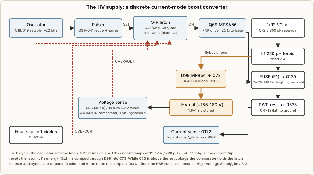
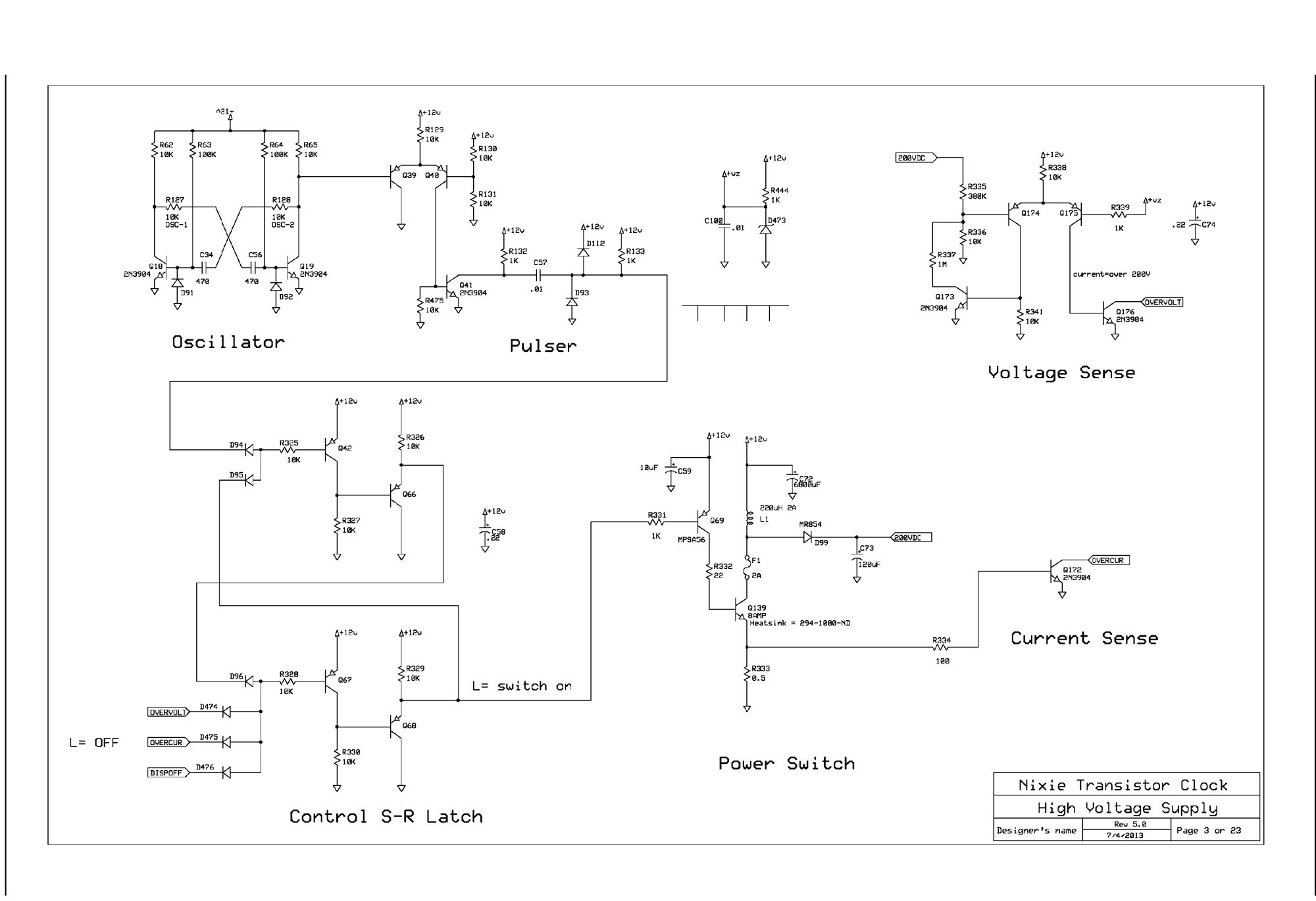
- Oscillator. Q18 and Q19 form a transistor astable. The manual asks for about 22 kHz, tuned if necessary by swapping the 470 pF and 0.001 µF timing capacitors.1
- Pulser and latch. Each oscillator edge becomes a short pulse (Q39–Q41, C57) that sets a set-reset latch built from two transistor pairs (Q42/Q66, Q67/Q68). Three diode-OR’d reset inputs, OVERVOLT, OVERCUR and DISPOFF, override it.
- The switch. When set, the latch turns on Q69 (MPSA56, PNP), which drives the base of Q139, a TO-220 power Darlington, through 22 Ω. Q139 sits on a heatsink.
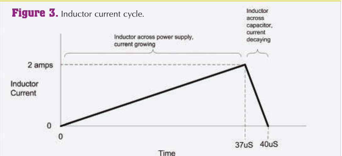
- The inductor. With Q139 on, current ramps up in L1, a 220 µH toroid, from the “+12 V” rail and its own 6,800 µF reservoir (C72), at 12–17 V ÷ 220 µH ≈ 54–77 mA per µs: about 37 µs to reach 2 A at 12 V, as the designer’s own figure shows (Figure 2.3).
- The current trip. Q139’s emitter returns through R333, the PWR resistor (0.47 Ω in the kit). When the voltage across it reaches one base-emitter drop, Q172 conducts and resets the latch.
- Delivery. Q139 turns off, L1’s voltage flies up, and its energy (½LI²) flows through D99 (MR854, 3 A 400 V) into C73, 120 µF, the HV reservoir. The manual quotes about 2.2 µs for the current to fall back to zero.1
- Regulation. A divider of the SNS resistor (R335) over 10 kΩ feeds a transistor comparator (Q174/Q175) referenced to a 4.7 V zener. Above the set voltage it holds the latch reset and cycles are skipped. A 1 MΩ resistor and Q173 add hysteresis.
- Hour shut-off. DISPOFF holds the latch reset during any hour whose shut-off diode is loaded (Volume 1, §1.4).
- Fuse. A pico fuse (the FUSE position, F1) sits in series with Q139’s collector.
2.2 Setting the voltage
The comparator trips when the divided output equals the zener voltage:
V_HV = V_z × (R_SNS + 10 kΩ) / 10 kΩ

R_SNS    V_z = 4.5 V    V_z = 4.7 V
348 k    161 V          168 V
357 k    165 V          173 V
390 k    180 V          188 V
The kit supplies all three SNS values because the zener’s voltage varies from part to part. The manual’s procedure fits 357 kΩ, expects “about 160 volts, give or take 20”, and swaps to 348 kΩ if the result is above 167 V or 390 kΩ if below 160 V.1 Its own expectation of about 165 V from 357 kΩ implies the zener runs nearer 4.5 V than its 4.7 V nominal, which is normal: it is biased at only about 7 mA (12 V − 4.7 V through 1 kΩ). The schematic’s “380K” for R335 is superseded by this three-value set.
The manual recommends staying at about 165 V: “The higher the voltage, the more power spent in the NIXIE displays, so, over 165 volts, your transformer may overheat.”1
2.3 Findings
Table 1 — 2.3 Findings
| # | Finding | Detail | What to do |
|---|---|---|---|
| 1 | Stored energy is high | C73 holds ½ × 120 µF × V²: 1.63 J at 165 V, 1.94 J at 180 V | Treat it with respect (§2.5); consider a bleeder |
| 2 | Slow discharge | Only the 367 kΩ divider bleeds C73: τ ≈ 44 s, so about 1½ minutes from 145 V to 20 V | Wait and measure; the manual says “that can take minutes” |
| 3 | A dark display is not a safe board | In shut-off hours the supply stops, the tubes go dark below about 145 V, and C73 then holds that voltage for minutes | Never read dark tubes as “off” |
| 4 | Manual’s arithmetic | Says 2.4 J at 180 V and 5,454 pulses to charge (correct: 1.94 J, about 4,400 pulses), and “about 18 uSeconds to reach 2 amps” (correct: about 37 µs at 12 V, as the 2012 article gives) | Minor; corrected here |
| 5 | Peak current vs the schematic | One V_BE across 0.47 Ω is about 1.3–1.5 A on paper, but the designer reports “about two amps detection” and his traces show about 2 A; the manual’s bring-up trace shows 2.5 A | Expect about 2 A; measure it at bring-up (§2.4) |
| 6 | L1 rating vs peak | L1 is a 2 A toroid; if peaks really reach 2.5 A it runs past its rating | If your measured peak is above 2 A, use an inductor with saturation current ≥ 3 A |
| 7 | Q139 is not identified | Schematic: “8AMP”; BOM: “Transistor, NPN Power, TO-220”; manual: “actually a Darlington” | Must be a high-voltage Darlington: MJE5742 (400 V, 8 A) is the safe choice; a 200 V part such as the BU806 is too marginal |
| 8 | C73’s voltage rating is not stated | BOM: “Capacitor, 120uF” | 250 V minimum, 105 °C, if you source it |
| 9 | Fuse rating disagrees | Schematic: F1 2 A; BOM: “Fuse, 3A, Fast, pico” | Use the BOM’s 3 A (the BOM was updated in 2015, after the 2013 schematic) |
| 10 | PWR value disagrees | Schematic: R333 0.5 Ω; BOM and procedure: 0.47 Ω | Use 0.47 Ω |
| 11 | Tubes run below their typical current | 0.9 mA at 165 V against the IN-12A’s 2.5–3.5 mA typical | A deliberate trade-off; see §2.6 |
1 to 3: the energy. The relay clock’s supply stores about 0.07 J in 4.7 µF; this one stores about 25 times as much in 120 µF, enough to give a seriously dangerous shock. The tubes help drain it when power is removed, but only until the voltage falls below what keeps them lit, about 145 V. From there only the divider bleeds it, with a time constant of 120 µF × 367 kΩ ≈ 44 s:
t(145 V → 20 V) = 44 s × ln(145 / 20) ≈ 87 sThe manual says so plainly: “you must wait for the 165 volts to decay below 20 volts before touching the board, and that can take minutes.”1 Finding 3 is the trap: during shut-off hours the board looks off while C73 sits at about 145 V.
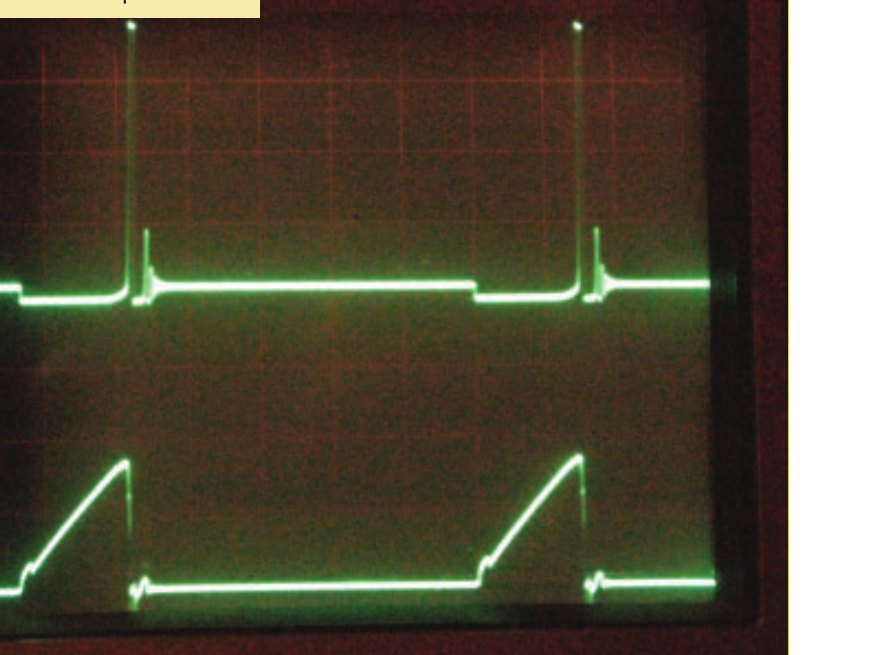
5 and 6: the peak current. The current trip is a single transistor whose base is driven from the PWR resistor through 100 Ω, so it begins to conduct at about 0.6–0.7 V across 0.47 Ω, 1.3–1.5 A. Yet the designer’s 2012 article says the 0.5 Ω sense resistor “results in about two amps detection”, his scope traces show the current near 2 A at turn-off (Figure 2.4), and the manual’s bring-up section shows a trace reaching 2.5 A.12 The difference is turn-off delay: after the trip fires, the latch has to flip and a Darlington has to come out of saturation, and all the while the inductor current keeps climbing at 54–77 mA/µs. That is plausible, and the bring-up procedure already includes looking at the current on a scope (§2.4). It matters because L1 is rated 2 A: a toroid pushed past its saturation current loses inductance, and the current then rises steeply, stressing Q139, D99 and the fuse.
2.4 Bringing it up: follow the manual exactly
The manual’s procedure is a model of how to bring up a dangerous supply, and it is worth following to the letter.1 It builds the HV supply last, after all the logic works, then:
- Load the HV parts except the FUSE, PWR and SNS positions.
- Fit stand-ins: a 47 kΩ in SNS (sets about 25.5 V), 10 Ω in PWR (limits the current to about 70 mA) and 22 Ω in FUSE (protects Q139).
- Power for under a second and read C73. About 25.5 V proves the oscillator, pulser, latch, current trip and regulator all work, safely. Over 30 V: unplug and debug.
- Fit the real 0.47 Ω PWR resistor and the 3 A fuse, confirm 25.5 V again, and scope the current across the PWR resistor: 2 A reads 0.94 V. This is the moment to check findings 5 and 6.
- Fit the 357 kΩ SNS resistor. Now the board is lethal. Bump the power and confirm the voltage settles at about 165 V; adjust SNS as in §2.2.
2.5 An optional bleeder
The one change worth considering is a bleeder resistor across C73, to bring the discharge time down from a minute and a half to something you will actually wait for. It is not on the board; it would be soldered across C73’s leads on the solder side.
R_bleed = 150 kΩ, in parallel with the 367 kΩ divider → 106 kΩ
τ = 120 µF × 106 kΩ ≈ 12.8 s;   145 V → 20 V in about 25 s
dissipation at 165 V: 165² / 150 k ≈ 0.18 W
Use a part rated at least 1 W and 350 V working (or two 75 kΩ 1/2 W resistors in series), since a small resistor’s voltage rating can be lower than the rail. The extra 0.18 W load is about 1% of the clock’s consumption. A bleeder does not replace measuring before touching; it shortens the wait.
2.6 Tube current, and the transformer
At the recommended 165 V, each lit digit draws about 0.9 mA through its 22 kΩ cathode resistor (Volume 1, §1.6), well under the IN-12A’s typical 2.5–3.5 mA.3 The designer limits it on purpose: the manual warns the 12 VAC transformer may overheat above 165 V. The kit’s finished clock (Volume 1, Figure 1.0) shows bright, fully formed digits, so the low current clearly works with the supplied tubes.
If your digits look patchy or thin:
Table 2 — If your digits look patchy or thin
| Option | Effect | Cost |
|---|---|---|
| SNS 390 kΩ (about 180 V) | 1.6 mA per digit | More HV power, more stored energy (1.94 J); check the transformer |
| Cathode resistors 15 kΩ at 165 V | 1.3 mA per digit | 45 resistors to change |
| A larger 12 VAC transformer | Headroom for either change | The kit’s adapter draws about 1.2 A (14.4 VA); a 2 A (24 VA) unit gives margin |
Build it as designed first. After an hour of running, feel the transformer. If it is only warm, there is room to raise the current; if it is hot, leave it alone or fit a larger transformer.
My build: I am fitting the 150 kΩ bleeder across C73 for safety.
2.7 The designer’s account (Nuts & Volts, April 2012)
Keith Bayern described designing this supply in “Return to Transistor Land”, Nuts & Volts, April 2012.2 The article adds the reasoning the manual leaves out:
- The budget. Six IN-12A tubes and five NE-2 neons needed, by his estimate, 180 V at 25 mA, all from the clock’s unregulated 12 V.
- The cycle. At 12 V across 220 µH the current rises at 54.5 kA/s, reaching 2 A in about 37 µs; discharging at 168 V, it falls to zero in 2.6 µs. A full cycle takes about 40 µs, so the oscillator must run slower than 25 kHz, and he chose about 22 kHz to stay above the “whine” humans hear below 20 kHz. He tried inductors from 20 to 500 µH before settling on 220 µH.
- Why the zener. His first version used the 12 V rail as the regulator’s reference. That put 60 Hz ripple on the 180 V output, and caused a slow oscillation, about three times a second: a load pulled the 12 V down, the detector wrongly switched the supply off, the 12 V recovered, and the supply switched back on. The 4.7 V zener reference cured both.
- The bring-up he used is the one the manual now prescribes: a large sense resistor first (the current trip working at 20 mA), then the real 0.5 Ω, and a 20 V regulation point before the full voltage.
- A sound to expect. Because cycles are skipped at random, the inductor’s windings move and make “a whooshing sound”; he suggests a potted inductor would help. It is worth knowing before mistaking it for a fault.
2.8 References (Vol 2)
Footnotes
-
Keith Bayern, KABtronics, Nixie-Transistor Clock Assembly Manual, document 1.7 for PCB version 5, 2016: High Voltage Power Supply and High Voltage Switcher build steps, theory of operation, circuit description (the inductor arithmetic), schematic sheet 3 (Rev 5.0, 2013), https://tube-clock.com/neon_man.pdf. ↩ ↩2 ↩3 ↩4 ↩5 ↩6 ↩7 ↩8
-
Keith Bayern, “Return to Transistor Land,” Nuts & Volts, April 2012, pp. 36–39, https://www.nutsvolts.com/magazine/article/april2012_Bayern. Checked against the next six issues (May–October 2012): no published letters or corrections. ↩ ↩2
-
IN-12 nixie tube datasheet (English translation), central Library
in-12-nixie-tubes-datasheet-eng. ↩
Comments (0)